

Product type
 Contact Information
+86 755 89660635
+86 189 2461 3736

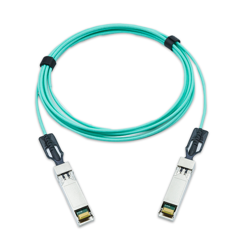
SFP+ 10Gbps Active Optical Cable
XCSS10A85xxDC
10Gbps SFP+ Active Optical Cable
Features
nHot-pluggable SFP+ cable ends
nSupport 10.3125Gbps bit rate
nAvailable in lengths up to 300m
nPower Dissipation <1W
nSingle +3.3V power supply
nOperating Case temperature range 0°C to 70°C
nRoHS-6 compliant
nCompliant with SFF-8431
nCompliant with SFF-8432
Applications
n10G Ethernet
nData Center
Ordering information
Part No. | Reach | Data Rate | Temp. |
XCSS10A8503DC | 3m | 10.3125Gpbs | 0°C to 70°C |
XCSS10A8505DC | 5m | 10.3125Gpbs | 0°C to 70°C |
XCSS10A8507DC | 7m | 10.3125Gpbs | 0°C to 70°C |
XCSS10A8510DC | 10m | 10.3125Gpbs | 0°C to 70°C |
XCSS10A8515DC | 15m | 10.3125Gpbs | 0°C to 70°C |
XCSS10A8520DC | 20m | 10.3125Gpbs | 0°C to 70°C |
XCSS10A853HDC | 300m | 10.3125Gpbs | 0°C to 70°C |
More detail product selection and cable lengths, please contact Zkosemi.
Description
XCSS10A85xxDC SFP+ active optical cables are designed for use in 10G-Ethernet links. They are compliant with SFF-8431, and the mechanical SFP+ plug is compatible with SFF-8432
Absolute Maximum Ratings
Parameter | Symbol | Min. | Typical | Max. | Unit | Note |
Power Supply Voltage | VCC | 0 | 3.6 | V | ||
Storage Temperature | Ts | -40 | +85 | 。C | ||
Relative Humidity | RH | 5 | 85 | % | Non-condensing | |
Operating Case Temperature | Tc | 0 | +70 | °C |
Electrical Characteristics
Parameter | Symbol | Min. | Typical | Max. | Unit | Note |
Power Supply Voltage | VCC | 3.135 | 3.3 | 3.465 | V | |
Power Dissipation | PD | 1 | W | |||
Power Supply Current | Icc | 310 | mA | |||
Data Rate | 1 | 10.3125 | 10.5 | Gbps | ||
Clock Rate-I2C | 400 | kHz | ||||
Transmitter | ||||||
Input Differential impedance | ZIN | 100 | ohm | |||
Differential data input swing | VIN | 180 | 700 | mV | ||
Transmit Disable Voltage | VDIS | 2 | VCC+0.3 | V | ||
Transmit Enable Voltage | VEN | 0 | 0.8 | V | ||
Transmit Fault Assert Voltage | 2 | VCC+0.3 | V | |||
Transmit Fault De-Assert Voltage | 0 | 0.8 | V | |||
Receiver | ||||||
Output Differential impedance | Zout | 100 | ohm | |||
Differential data Output Swing | Vout | 300 | 850 | mV | ||
Rx_LOS Output Voltage-High | 2 | VCC+0.3 | V | |||
Rx_LOS Output Voltage-Low | 0 | 0.8 | V | |||
General Specifications
Parameter | Symbol | Min. | Typical | Max. | Unit | Note | |
Bit Rate | BR | 1 | 10.3125 | 10.5 | Gbps | ||
Bit Error Ratio | BER | E-12 | PRBS31 | ||||
Maximum Supported Distances | |||||||
Fiber Type | Bandwidth (850nm) | ||||||
50um | 2000MHz*km | 300 | m | OM3 | |||
Pin Assignment:

Pin Descriptions
PIN | Symbol | Name / Description | Note |
1 | VEET | Transmitter Ground (Common with Receiver Ground) | 1 |
2 | TX_Fault | Transmitter Fault | 2 |
3 | TX_Dis | Transmitter Disable | 3 |
4 | SDA | 2-Wire Serial Interface Data Line | 4 |
5 | SCL | 2-Wire Serial Interface Clock | 4 |
6 | MOD_ABS | Module Definition, Grounded in the module | --- |
7 | RS0 | Receiver Rate Select (not used) | --- |
8 | RX_LOS | Receiver Loss of Signal Indication | 5 |
9 | RS1 | Transmitter Rate Select (not used) | --- |
10 | VEER | Receiver Ground (Common with Transmitter Ground) | 1 |
11 | VEER | Receiver Ground (Common with Transmitter Ground) | 1 |
12 | RD- | Receiver Inverted Data Output | 6 |
13 | RD+ | Receiver Data Output | 6 |
14 | VEER | Receiver Ground (Common with Transmitter Ground) | 1 |
15 | VCCR | Receiver Power | 7 |
16 | VCCT | Transmitter Power | 7 |
17 | VEET | Transmitter Ground (Common with Receiver Ground) | 1 |
18 | TD+ | Transmitter Non-Inverted Data Input | 6 |
19 | TD- | Transmitter Inverted Data Input | 6 |
20 | VEET | Transmitter Ground (Common with Receiver Ground) | 1 |
Note1: Module ground pins GND are isolated from the module case.
Note2: The Tx_Fault output is an open collector/drain output, which should be pulled up with a 4.7k to 10k ohms resistor on the host board.
Note3: Transmitter output disabled on TDIS >2.0V or open, enabled on TDIS <0.8V.
Note4: Shall be pulled up with 4.7K-10Kohms to a voltage between 3.15V and 3.45V on the host board.
Note5: LOS is open collector output. Should be pulled up with 4.7 – 10k ohms on host board to a voltage between 2.0V and 3.6V. Logic 0 indicates normal operation; logic 1 indicates loss of signal.
Note6: VccR and VccT are the receiver and transmitter power supplies. They are defined as 3.3V ±5% at the SFP+ connector pin.
Note7: They areAC-coupled, differential lines with 100 Ω differential termination inside the module.
Mechanical Dimensions

Revision History
Revision | Initiated | Reviewed | Approved | DCN | Release Date |
V1.0 | Feynman | XX | XX | Released. | July 16, 2022 |
Important Notice
Performance figures, data and any illustrative material provided in this data sheet are typical and must be specifically confirmed in writing by Zkosemi before they become applicable to any particular order or contract. In accordance with the Zkosemi policy of continuous improvement specifications may change without notice. The publication of information in this data sheet does not imply freedom from patent or other protective rights of Zkosemi or others. Further details are available from any Zkosemi sales representative.