

Product type
 Contact Information
+86 755 89660635
+86 189 2461 3736

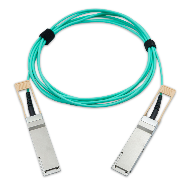
200G QSFP56 Active Optical Cable
XCQQ2HA85xxDC
200G QSFP56 Active Optical Cable
Features
lUp to 50Gbps data rate per channel by PAM4 modulation
lSupport 200GAUI‐4 electrical interface
lIntegrated 850nm VCSEL array and PD array
lSingle +3.3V power supply
lCase temperature range: 0 ~ +70℃
lHot‐pluggable QSFP form factor
lRoHS complaint
Applications
lData centers and Cloud Networks
lOther Optical Links
Standards
lIEEE 802.3cd
lSFF 8679
lCMIS4.0 or SFF8636
Product |
Electrial mode |
Protocol | Nomina Rate | Specifications |
Link | |||
Aggregate (Gbps) | Electrical Lanes (Gbaud) | ppm | High Speed Electrical | Pre‐FEC Max BER | ||||
200G‐AOC |
4X50 |
IEEE802.3c d |
212.5 |
26.5625 PAM4 |
±100 |
200GAUI‐4 |
2.4E‐4 |
0.5~100m |
Rev | Date | Modified by | Description |
A | Sep 5,2021 | Alan | Initial Release |
B | Feb 9,2022 | Alan | Update drawing |
Parameter | Symbol | Unit | Min | Max |
Case Operating Temperature | Top | ℃ | 0 | +70 |
Storage Temperature Range | Ts | ℃ | ‐40 | +85 |
Relative Humidity | RH | % | 0 | 85 |
Power Supply Voltage | Vcc | V | ‐0.5 | +3.6 |
Recommended Operating Conditions
Parameter | Symbol | Unit | Min | Typ | Max |
Operating Case Temperature Range | Tca | oC | 0 | / | 70 |
Power Supply Voltage | Vcc | V | 3.135 | 3.3 | 3.465 |
Electric Ports Definition
Parameter | Symbol | Unit | Min | Typ | Max | Notes |
Supply Voltage | VCC | V | 3.135 | 3.3 | 3.465 | |
Power Consumption | Pc | W | 4 | per end | ||
Transmitter | ||||||
Input Differential Impedance | RIN | Ω | 80 | 100 | 120 | |
Single Ended Data Input Swing | VIN | mVp‐p | 90 | 500 | ||
Transmit Disable Voltage | VDIS | V | 2 | VCCHOST | ||
Transmit Enable Voltage | VEN | V | VEE | VEE+0.8 | ||
Transmit Fault Assert Voltage | VFA | V | 2 | VCCHOST | ||
Transmit Fault De‐Assert Voltage | VFDA | V | VEE | VEE+0.8 | ||
Receiver | ||||||
Single Ended Data Output Swing | VOD | mVp‐p | 200 | 500 | ||
LOS Fault | VLOSFT | V | 2 | VCCHOST | ||
LOS Normal | VLOSNR | V | VEE | VEE+0.8 | ||
Differential termination mismatch | % | 10 | ||||
IIC communication | ||||||
IIC Clock frequency | ‐ | KHZ | / | 100 | 400 | |
clock stretching | ‐ | us | / | / | 500 | |
QSFP56 Connector and Pinout Description
The electrical interface to the transceiver is a 38 pins edge connector. The 38 pins provide high speed data, low speed monitoring and control signals, I2C communication, power and ground connectivity. The top and bottom views of the connector are provided below, as well as a table outlining the contact numbering, symbol and full description.

Pin | Symbol | Name/Description |
1 | GND | Ground |
2 | Tx2n | Transmitter Inverted Data Input |
3 | Tx2p | Transmitter Non-Inverted Data Input |
4 | GND | Ground |
5 | Tx4n | Transmitter Inverted Data Input |
6 | Tx4p | Transmitter Non-Inverted Data Input |
7 | GND | Ground |
8 | ModSelL | Module Select |
9 | ResetL | Module Reset |
10 | Vcc Rx | +3.3 V Power supply receiver |
11 | SCL | 2-wire serial interface clock |
12 | SDA | 2-wire serial interface data |
13 | GND | Ground |
14 | Rx3p | Receiver Non-Inverted Data Output |
15 | Rx3n | Receiver Inverted Data Output |
16 | GND | Ground |
17 | Rx1p | Receiver Non-Inverted Data Output |
18 | Rx1n | Receiver Inverted Data Output |
19 | GND | Ground |
20 | GND | Ground |
21 | Rx2n | Receiver Inverted Data Output |
22 | Rx2p | Receiver Non-Inverted Data Output |
23 | GND | Ground |
24 | Rx4n | Receiver Inverted Data Output |
25 | Rx4p | Receiver Non-Inverted Data Output |
26 | GND | Ground |
27 | ModPrsL | Module Present |
28 | IntL | Interrupt |
29 | Vcc Tx | +3.3 V Power supply transmitter |
30 | Vcc1 | +3.3 V Power Supply |
31 | LPMode | Low Power Mode |
32 | GND | Ground |
33 | Tx3p | Transmitter Non-Inverted Data Input |
34 | Tx3n | Transmitter Inverted Data Input |
35 | GND | Ground |
36 | Tx1p | Transmitter Non-Inverted Data Input |
37 | Tx1n | Transmitter Inverted Data Input |
38 | GND | Ground |

Standard Cable lengths for each PN
Part Number |
Description |
XCQQ2HA85xxDC | 200G QSFP56 SR4 AOC 3M |