

Product type
 Contact Information
+86 755 89660635
+86 189 2461 3736

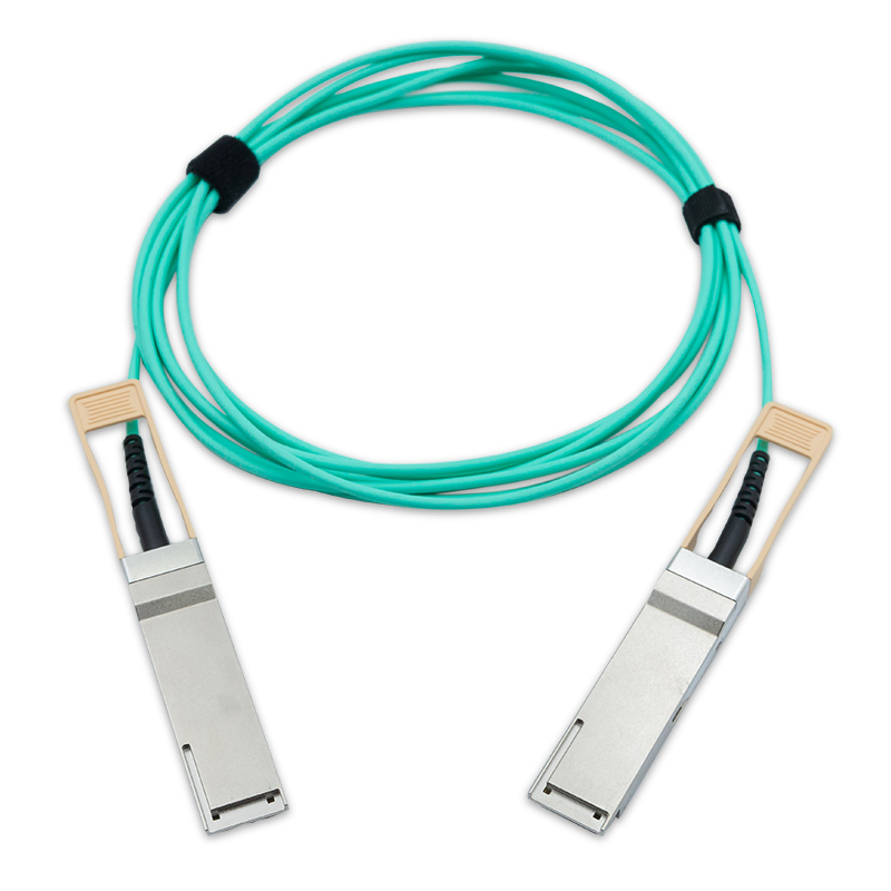
200G QSFP56 to 2x100G QSFP56 Active Optical Breakout Cable
ZK-QSFP56-2xQSFP56-AOC
200Gbps QSFP56 to 2x100Gbps QSFP56 Active Optical Breakout Cable
Features
n Supports IBTA InfiniBand HDR
n 200Gb/s HDR to 2x100Gb/s HDR100 data rate
n 4x 50Gb/s PAM4 modulation
n SFF-8665 compliant QSFP56 port
n SFF-8636 compliant I2C management
n Single 3.3V power supply
n Max 4.5W power dissipation each end, with retiming
n Operating case temp Commercial: 0°C to +70 °C
n Hot pluggable
n RoHS compliant
Applications
n 200Gb/s InfiniBand HDR systems
n Other optical links
Absolute Maximum Ratings
Parameter | Symbol | Min. | Typical | Max. | Unit | Notes |
Supply Voltage | Vcc3 | -0.5 | - | +3.6 | V | |
Storage Temperature | Ts | -5 | - | +75 | °C | |
Operating Humidity | RH | +5 | - | +85 | % | 1 |
Note:
1. No condensation
Recommended Operating Conditions
Parameter | Symbol | Min. | Typical | Max. | Unit | Notes | |
Operating Case Temperature | TC | 0 | - | +70 | °C | ||
Power Supply Voltage | Vcc | 3.14 | 3.3 | 3.47 | V | ||
Power dissipation (200G retiming on all lanes) | Pd200G | - | - | 4.5 | W | 1 | |
Power dissipation (100G retiming on all lanes) | Pd100G | - | - | 2.5 | W | 1 | |
Note:
1. Per terminal
Electrical Characteristics
Parameter | Symbol | Unit | Min | Typ | Max | Notes |
Transmitter | ||||||
Signaling rate (each lane) | SR | GBd | 26.5625 ± 100 ppm | |||
Differential data input voltage per lane | Vin,pp,diff | mV | 900 | - | - | |
Differential termination mismatchal | - | % | - | - | 10 | |
Single-ended voltage tolerance range | - | V | -0.4 | - | 3.3 | |
DC common mode voltage | - | mV | -350 | - | 2850 | |
Receiver | ||||||
Signaling rate (each lane) | SR | GBd | 26.5625 ± 100 ppm | |||
Differential output voltage | - | mV | - | - | 900 | |
Differential termination mismatch | - | % | - | - | 10 | |
Transition time (min, 20% to 80%) | - | ps | 9.5 | - | - | |
DC common mode voltage | - | mV | -350 | - | 2850 | |
Error Bit Rate | BER | - | - | - | 2.4E-4 | Note1 |
Note:
1. PRBS31Q@26.5625Gbd PAM4
Recommended Interface Circuit

Pin arrangement
Pin View
Pin Function Definitions
Pin | Symbol | Name/Description | Notes |
1 | GND | Ground | 1 |
2 | Tx2n | Transmitter Inverted Data Input | |
3 | Tx2p | Transmitter Non-Inverted Data Input | |
4 | GND | Ground | 1 |
5 | Tx4n | Transmitter Inverted Data Input | |
6 | Tx4p | Transmitter Non-Inverted Data Input | |
7 | GND | Ground | 1 |
8 | ModSelL | Module Select | |
9 | ResetL | Module Reset | |
10 | Vcc Rx | +3.3V Power Supply Receiver | |
11 | SCL | 2-wire serial interface clock | |
12 | SDA | 2-wire serial interface data | |
13 | GND | Ground | 1 |
14 | Rx3p | Receiver Non-Inverted Data Output | |
15 | Rx3n | Receiver Inverted Data Output | |
16 | GND | Ground | 1 |
17 | Rx1p | Receiver Non-Inverted Data Output | |
18 | Rx1n | Receiver Inverted Data Output | |
19 | GND | Ground | 1 |
20 | GND | Ground | 1 |
21 | Rx2n | Receiver Inverted Data Output | |
22 | Rx2p | Receiver Non-Inverted Data Output | |
23 | GND | Ground | 1 |
24 | Rx4n | Receiver Inverted Data Output | |
25 | Rx4p | Receiver Non-Inverted Data Output | |
26 | GND | Ground | 1 |
27 | ModPrsL | Module Present | |
28 | IntL | Interrupt | |
29 | Vcc Tx | +3.3V Power supply transmitter | |
30 | Vcc1 | +3.3V Power supply | |
31 | LPMode | Low Power Mode | |
32 | GND | Ground | 1 |
33 | Tx3p | Transmitter Non-Inverted Data Input | |
34 | Tx3n | Transmitter Inverted Data Input | |
35 | GND | Ground | 1 |
36 | Tx1p | Transmitter Non-Inverted Data Input | |
37 | Tx1n | Transmitter Inverted Data Input | |
38 | GND | Ground | 1 |
Note:
1. Circuit ground is internally isolated from chassis ground.
Monitoring Specification
Memory Map
Cable Length
Parameter | Value | Units |
Diameter | 3±0.2 | mm |
Minimum bend radius | 30 | mm |
Length tolerance | 1 m ≤length ≤ 4.5 m: +15 / -0
| cm |
5 m ≤length ≤ 14.5 m: +30 / -0
| cm | |
Length≥15.0 m +2% / -0 | m | |
Cable color | Aqua | |
Connectivity Schematic
200Gb/s Side | 100Gb/s Side |
Port 1 | |
TX1 | RX1 |
RX1 | TX1 |
TX2 | RX2 |
RX2 | TX2 |
Port 2 | |
TX3 | RX1 |
RX3 | TX1 |
TX4 | RX2 |
RX4 | TX2 |
Important Notice
Performance figures, data and any illustrative material provided in this data sheet are typical and must be specifically confirmed in writing by Zkosemi before they become applicable to any particular order or contract. In accordance with the Zkosemi policy of continuous improvement specifications may change without notice. The publication of information in this data sheet does not imply freedom from patent or other protective rights of Zkosemi or others. Further details are available from any Zkosemi sales representative.