

Product type
 Contact Information
+86 755 89660635
+86 189 2461 3736

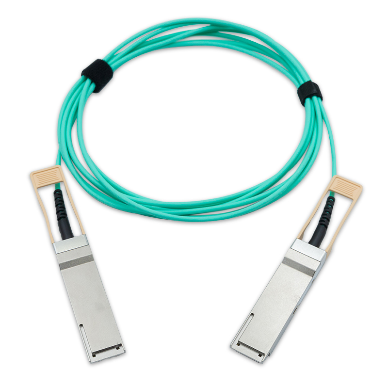
400G QSFP-DD Active Optical Cable
ZK-QDD-400G-AOC
400Gbps QSFP-DD Active Optical Cable
Features
n Data rate up to 425Gb/s (8x PAM4 53Gb/s)
n 850nm VCSEL laser and PIN receiver
n High speed I/O electrical interface (400GAUI-8)
n I2C interface with integrated Digital Diagnostic Monitoring (DDM)
n Single +3.3V power supply
n Power consumption less than 8W per end
n Low latency time with CDR solution
n Operating case temperature:0~+70°C
n Compliant to RoHS-10
Applications
n 400GBASE-SR8
Standards
n IEEE 802.3bs, IEEE 802.3cm
n QSFP-DD MSA Rev5.0
n CMIS5.0
Absolute maximum ratings (TC=25°C, unless otherwise noted)
Stresses in excess of the absolute maximum ratings can cause permanent damage to the device. These are absolute stress ratings only. Functional operation of the device is not implied at these or any other conditions in excess of those given in the operational sections of the data sheet. Exposure to absolute maximum ratings will cause permanent damage and/or adversely affect device reliability.
Parameter | Symbol | Min | Typical | Max | Unit | Notes |
Storage Temperature | TS | -40 | - | +85 | ºC | |
Maximum Supply Voltage | Vcc | -0.5 | - | 4.0 | V | |
Operating Relative Humidity | RH | + 15 | - | +85 | % | No condensation |
General specifications (TC=25°C, Unless Otherwise Noted)
Parameter | Symbol | Min | Typical | Max | Unit | Notes |
Operating Case Temperature | Tc | 0 | - | 70 | ºC | |
Power Supply Voltage | Vcc | 3.13 | 3.3 | 3.47 | V | |
Maximum Power Dissipation | PD | - | - | 8 | W | |
Lane Baud Rate | BRLANE | 53.125 | Gbps |
Pin Descriptions
Pad | Logic | Symbol | Description | Plug Seq4 | Notes |
1 | GND | Ground | 1B | 1 | |
2 | CML-I | Tx2n | Transmitter Inverted Data Input | 3B | |
3 | CML-I | Tx2p | Transmitter Non-Inverted Data Input | 3B | |
4 | GND | Ground | 1B | 1 | |
5 | CML-I | Tx4n | Transmitter Inverted Data Input | 3B | |
6 | CML-I | Tx4p | Transmitter Non-Inverted Data Input | 3B | |
7 | GND | Ground | 1B | 1 | |
8 | LVTTL-I | ModSelL | Module Select. | 3B | |
9 | LVTTL-I | ResetL | Module Reset. | 3B | |
10 | VccRx | +3.3V Power Supply Receiver | 2B | 2 | |
11 | LVCMOS-I/O | SCL | 2-wire serial interface clock | 3B | |
12 | LVCMOS-I/O | SDA | 2-wire serial interface data | 3B | |
13 | GND | Ground | 1B | 1 | |
14 | CML-O | Rx3p | Receiver Non-Inverted Data Output | 3B | |
15 | CML-O | Rx3n | Receiver Inverted Data Output | 3B | |
16 | GND | Ground | 1B | 1 | |
17 | CML-O | Rx1p | Receiver Non-Inverted Data Output | 3B | |
18 | CML-O | Rx1n | Receiver Inverted Data Output | 3B | |
19 | GND | Ground | 1B | 1 | |
20 | GND | Ground | 1B | 1 | |
21 | CML-O | Rx2n | Receiver Inverted Data Output | 3B | |
22 | CML-O | Rx2p | Receiver Non-Inverted Data Output | 3B | |
23 | GND | Ground | 1B | 1 | |
24 | CML-O | Rx4n | Receiver Inverted Data Output | 3B | |
25 | CML-O | Rx4p | Receiver Non-Inverted Data Output | 3B | |
26 | GND | Ground | 1B | 1 | |
27 | LVTTL-O | ModPrsL | Module Present. | 3B | |
28 | LVTTL-O | IntL | Interrupt. | 3B | |
29 | VccTx | +3.3V Power supply transmitter | 2B | 2 | |
30 | Vcc1 | +3.3V Power supply | 2B | 2 | |
31 | LVTTL-I | LPMode | Low Power Mode | 3B | |
32 | GND | Ground | 1B | 1 | |
33 | CML-I | Tx3p | Transmitter Non-Inverted Data Input | 3B | |
34 | CML-I | Tx3n | Transmitter Inverted Data Input | 3B | |
35 | GND | Ground | 1B | 1 | |
36 | CML-I | Tx1p | Transmitter Non-Inverted Data Input | 3B | |
37 | CML-I | Tx1n | Transmitter Inverted Data Input | 3B | |
38 | GND | Ground | 1B | 1 | |
39 | GND | Ground | 1A | 1 | |
40 | CML-I | Tx6n | Transmitter Inverted Data Input | 3A | |
41 | CML-I | Tx6p | Transmitter Non-Inverted Data Input | 3A | |
42 | GND | Ground | 1A | 1 | |
43 | CML-I | Tx8n | Transmitter Inverted Data Input | 3A | |
44 | CML-I | Tx8p | Transmitter Non-Inverted Data Input | 3A | |
45 | GND | Ground | 1A | 1 | |
46 | Reserved | For future use | 3A | 3 | |
47 | VS1 | Module Vendor Specific 1 | 3A | 3 | |
48 | VccRx1 | 3.3V Power Supply | 2A | 2 |
Notes:
1. QSFP-DD uses common ground (GND) for all signals and supply (power). All are common within the QSFP-DD
2. module and all module voltages are referenced to this potential unless otherwise noted. Connect these directly to the host board signal-common ground plane.
3. VccRx, VccRx1, Vcc1, Vcc2, VccTx and VccTx1 shall be applied concurrently. Requirements defined for the host side of the Host Card Edge Connector are listed in Table 7. VccRx, VccRx1, Vcc1, Vcc2, VccTx and VccTx1 may be internally connected within the module in any combination. The connector Vcc pins are each rated for a maximum current of 1000 mA.
4. All Vendor Specific, Reserved, No Connect and ePPS (if not used) pins may be terminated with 50 Ohms to ground on the host. Pad 65 (No Connect) shall be left unconnected within the module. Vendor specific and Reserved pads shall have an impedance to GND that is greater than 10 kOhms and less than 100 pF
5. Plug Sequence specifies the mating sequence of the host connector and module. The sequence is 1A, 2A, 3A, 1B, 2B, 3B (see Figure 2 for pad locations). Contact sequence A will make, then break contact with additional QSFP-DD pads. Sequence 1A,1B will then occur simultaneously, followed by 2A,2B, followed by 3A, 3B
Digital Diagnostic Functions
Parameter | Symbol | Min | Typical | Max | Units | Notes |
Bit Rate (per lane) | BR | 53.125 | Gb/s | |||
Electrical Bit Error Rate (per lane) | BER | 1E-6 | PRBS31Q |
Electrical Characteristics
Parameter | Symbol | Min | Typical | Max | Units | Notes | |
Receiver electrical output characteristics at TP4 | |||||||
Signaling rate per lane | 26.5625 | GBd | |||||
AC common-mode output voltage(RMS) |
- | 17 .5 | mV | ||||
Differential peak-to-peak output voltage | 90 0 | mV | |||||
Near-end ESMW (Eye symmetry mask width) | 0.265 | UI | |||||
Near-end Eye height, differential | 70 | mV | |||||
Far-end ESMW (Eye symmetry mask width) | 0.2 | UI | |||||
Far-end Eye height, differential | 30 | mV | |||||
Far-end pre-cursor ISI ratio | -4.5 | 2. 5 | % | ||||
Differential output return loss | 9.5 - 0.37f | dB | 0.01 - 8 GHz | ||||
4.75 -7.4log 10 (f/14) | dB | 8 - 19 GHz | |||||
Common to differential mode conversion return loss | 22-20(f/25.78) | dB | 0.01 -12.89 GHz | ||||
15 -6log 10 (f/25.78) | dB | 12.89 - 19 GHz | |||||
Differential termination mismatch | 10 | % | |||||
Transition time (min, 20% to 80%) | 9.5 | ps | |||||
DC common mode voltage | -350 | 2850 | mV | ||||
Transmitter electrical input characteristics at TP1 | |||||||
Signaling rate, per lane | 26.5625 | GBd | |||||
Differential pk-pk input voltage tolerance | 900 | mV | |||||
Differential input return loss | 9.5 - 0.37f | dB | 0.01 - 8 GHz | ||||
4.75 -7.4log 10(f/14) | dB | 8 - 19 GHz | |||||
Differential to common mode input return loss | 22-20(f/25.78) | dB | 0.01 -12.89 GHz | ||||
15 -6log 10 (f/25.78) | dB | 12.89 - 19 GHz | |||||
Differential termination mismatch | 10 | % | |||||
Module stressed input test | Per Section 120E.3.4.1, IEEE802.3bs | ||||||
Single-ended voltage tolerance range | -0.4 | 3.3 | V | ||||
Common-mode voltage | -350 | 2850 | mV | ||||
Low Speed Control And Sense Signals

Memory Map
Digital Diagnostic Specification
Parameter | Symbol | Accuracy | Units | Notes |
Transceiver Case Temperature | DMI_TEMP | ±5 | ℃ | Over operating temp |
Supply voltage monitor absolute error | DMI _VCC | ±3% | V | Full operating range |
Channel Bias current monitor | DMI_IBIAS | ±10% | mA | Per channel |
Channel RX power monitor absolute error | DMI_RX | ±3 | dB | Per channel |
Channel TX power monitor absolute error | DMI_TX | ±3 | dB | Per channel |
Mechanical Specifications
Unit: mm 
Important Notice
Performance figures, data and any illustrative material provided in this data sheet are typical and must be specifically confirmed in writing by Zkosemi before they become applicable to any particular order or contract. In accordance with the Zkosemi policy of continuous improvement specifications may change without notice. The publication of information in this data sheet does not imply freedom from patent or other protective rights of Zkosemi or others. Further details are available from any Zkosemi sales representative.