

Product type
 Contact Information
+86 755 89660635
+86 189 2461 3736

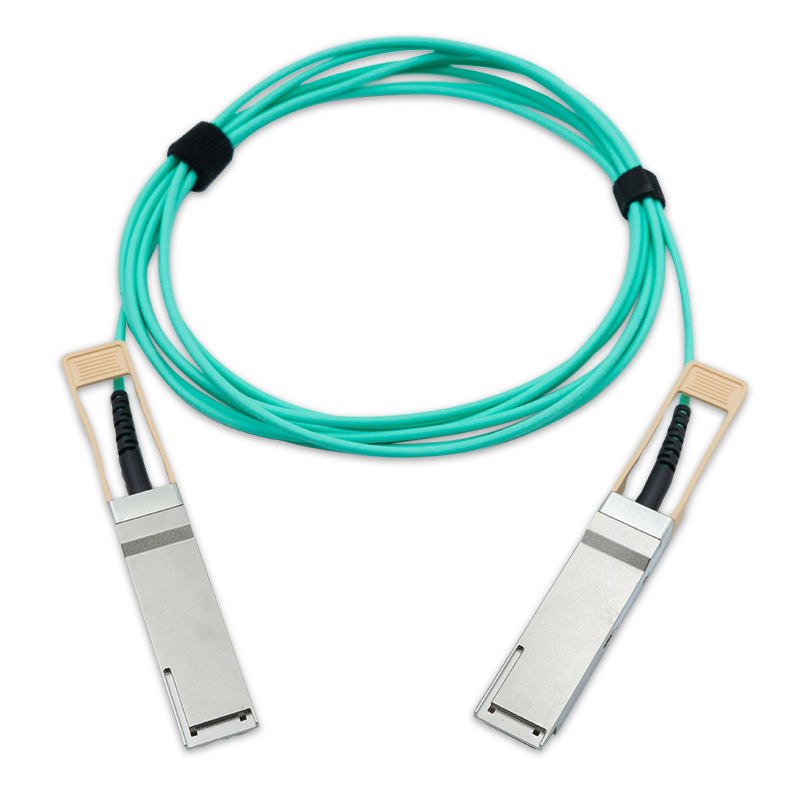
200Gbps QSFP56 Active Optical Cable
ZK-QSFP56-200G-AOC
200Gbps QSFP56 Active Optical Cable
Features
n Hot-pluggable QSFP56 form factor
n Compliant with IEEE 802.3cd and IEEE 802.bs
n Management interface based on CMIS 4.0 or updated version
n Optical Interface: 53.125 Gbps (PAM4) x 4
n Electrical Interface: 53.125 Gbps (PAM4) x 4
n Up to 100m over OM4 MMF with FEC
n Case operating temperature: 0℃ to +70℃
n Single 3.3V power supply
n Power consumption: 4.5W Max.
n RoHS compliant
Applications
n 200G Ethernet
n Data center
Description
The QSFP56-200G-AOC is a Hot-Pluggable, Multi-Mode fiber for 200G short range of datacom interconnnection. Using VCSEL devices for 4 lanes,each electrical lane convert into optical lanes at 53.125Gbps giving an aggregated data rate of 212Gbps .It allows communication up to 70m using OM3 fiber or 100m using OM4 fiber with FEC. Compliant with the Common Management Interface Specification and MSA. This module incorporates proven circuit and VCSEL technology to provide reliable long life, high performance, and consistent service.
Recommended Power Supply Filter
Absolute Maximum Ratings
Parameter | Symbol | Min. | Max. | Unit | Note |
Supply Voltage | V cc | -0.5 | 3.6 | V | |
Storage Temperature | TS | -40 | 85 | °C | |
Relative Humidity | RH | 5 | 85 | % | |
Damage Threshold | 5 | dBm | 5 |
Recommended Operating Conditions
Parameter | Symbol | Min. | Typ | Max. | Unit | Note |
Electrical Signal Rate, each lane | 26.5625±100 ppm | GBd | ||||
Optical Signal Rate, each lane | 26.5625±100 ppm | GBd | ||||
Supply Voltage | V cc | 3.135 | 3.3 | 3.465 | V | |
Operating Case Temp. | Tc | 0 | - | 70 | °C | |
Power Consumption | Pc | 4.5 | W | |||
Link Distance with OM3 | Dl | 0.5 | 70 | m | ||
Link Distance with OM4 | D2 | 0.5 | 100 | m | ||
Optical Characteristics (Under Recommended Operating Conditions)
Parameter | Symbol | Min | Typ | Max | Unit | Note |
Transmitter | ||||||
Signaling rate, each lane (range) | 26.5625 ± 100 ppm | GBd | ||||
Modulation format | PAM4 | |||||
Center wavelength (range) | λ | 840 | - | 865 | nm | |
RMS spectral width | 0.65 | nm | 1 | |||
Average launch power, each lane | P | -6.5 | 4 | dBm | ||
OMAouter, each lane | POMA | -4.5 | 3 | dBm | 2 | |
Launch power in OMAouter minus TDECQ | -5.9 | dBm | ||||
Transmitter and dispersion eye closure for PAM4 (TDECQ), each lane | 4.5 | dB | ||||
Average launch power of OFF transmitter, each lane | P off | -30 | dBm | |||
Extinction ratio, each lane | ER | 3 | dB | |||
RIN21OMA | RIN | -128 | dB/Hz | |||
Optical return loss tolerance | 12 | dB | ||||
Receiver | ||||||
Signaling rate, each lane (range) | 26.5625 ± 100 ppm | GBd | ||||
Modulation format | PAM4 | |||||
Center wavelength (range) | λ | 840 | - | 865 | nm | |
Damage Threshold | 5 | dBm | 5 | |||
Average receive power, each lane | -8.4 | - | 4 | dBm | 6 | |
Receive power, each lane (OMAouter) | ROMA | 3 | dBm | |||
Receiver reflectance | -12 | dB | ||||
Receiver sensitivity (OMAouter), each lane | SEN | max(-6.5, SECQ-7.9) | dBm | 8 | ||
LOS Assert | -30 | -13 | dBm | |||
LOS De-Assert | -11 | dBm | ||||
LOS Hysteresis | 0.5 | dB | ||||
Note:
1. RMS spectral width is the standard deviation of the spectrum.
2. Even if the TDECQ <1.4 dB, the OMA (min) has to exceed this value.
3. Ceq is a coefficient defined in 121.8.5.3, which accounts for the reference equalizer noise enhancement.
4. If measured into type A1a.2 or type A1a.3, or A1a.4, 50 μm fiber, in accordance with IEC 61280-1-4:2009
5. The receiver shall be able to tolerate, without damage, continuous exposure to an optical input signal having this average power level on one lane. The receiver does not have to operate correctly at this input power.
6. Average receive power, each lane (min) is not the principal indicator of signal strength. A received power below this value cannot be compliant; however, avalue above this does not ensure compliance.
7. Measured with conformance test signal at TP3 (see IEEE802.3 138.8.10) for the BER specified in 138.1.1.
8. Receiver sensitivity is optional and is defined for a transmitter with a value of SECQ up to 4.5 dB.
Electrical Characteristics (Under Recommended Operating Conditions)
Parameter | TestPoint | Min | Typ | Max | Unit | Note |
High Speed Electrical Input Characteristics | ||||||
Signaling rate per lane | TP1 | 26.5625±100ppm | GBd | |||
Differential pk-pk input voltage tolerance | TP1a | 900 | mV | 1 | ||
Single-ended voltage tolerance | TP1a | -0.4 | 3.3 | V | ||
DC common mode voltage | TP1 | -350 | 2850 | mV | 2 | |
High Speed Electrical Output Characteristics | ||||||
Signaling rate per lane | TP4 | 26.5625±100ppm | GBd | |||
AC common-mode output voltage (RMS) | TP4 | 17.5 | mV | |||
Differential peak-to-peak output voltage | TP4 | 900 | mV | |||
Near-end ESMW (Eye symmetry mask width) | TP4 | 0.265 | UI | |||
Near-end Eye height, differential | TP4 | 70 | mV | |||
Far-end ESMW (Eye symmetry mask width) | TP4 | 0.2 | UI | |||
Far-end Eye height, differential | TP4 | 30 | mV | |||
DC common mode voltage | TP4 | -350 | 2850 | mV | 2 | |
Note:
1. With the exception to IEEE802.3bs 120E.3.1.2 that the pattern is PRBS31Q or scrambled idle.
2. DC common mode voltage generated by the host. Specification includes effects of ground offset voltage.
Digital Diagnostic Monitor Accuracy
The following characteristics are defined over recommended operating conditions.
Parameter | Accuracy | Unit | Note |
Measured transceiver temperature | ±3 | ℃ | |
Measured transceiver supply voltage | ±3 | % | |
Measured Tx bias current | ±10 | % | |
Measured Tx output power | ±3 | dB | |
Measured Rx received average optical power | ±3 | dB |
Pin Description
Pin | Symbol | Name/Description | Notes |
1 | GND | Ground | 1 |
2 | Tx2n | Transmitter Inverted Data Input | |
3 | Tx2p | Transmitter Non-Inverted Data Input | |
4 | GND | Ground | 1 |
5 | Tx4n | Transmitter Inverted Data Input | |
6 | Tx4p | Transmitter Non-Inverted Data Input | |
7 | GND | Ground | 1 |
8 | ModSelL | Module Select | |
9 | ResetL | Module Reset | |
10 | Vcc Rx | +3.3V Power Supply Receiver | |
11 | SCL | 2-wire serial interface clock | |
12 | SDA | 2-wire serial interface data | |
13 | GND | Ground | 1 |
14 | Rx3p | Receiver Non-Inverted Data Output | |
15 | Rx3n | Receiver Inverted Data Output | |
16 | GND | Ground | 1 |
17 | Rx1p | Receiver Non-Inverted Data Output | |
18 | Rx1n | Receiver Inverted Data Output | |
19 | GND | Ground | 1 |
20 | GND | Ground | 1 |
21 | Rx2n | Receiver Inverted Data Output | |
22 | Rx2p | Receiver Non-Inverted Data Output | |
23 | GND | Ground | 1 |
24 | Rx4n | Receiver Inverted Data Output | |
25 | Rx4p | Receiver Non-Inverted Data Output | |
26 | GND | Ground | 1 |
27 | ModPrsL | Module Present | |
28 | IntL | Interrupt | |
29 | Vcc Tx | +3.3V Power supply transmitter | |
30 | Vcc1 | +3.3V Power supply | |
31 | LPMode | Low Power Mode | |
32 | GND | Ground | 1 |
33 | Tx3p | Transmitter Non-Inverted Data Input | |
34 | Tx3n | Transmitter Inverted Data Input | |
35 | GND | Ground | 1 |
36 | Tx1p | Transmitter Non-Inverted Data Input | |
37 | Tx1n | Transmitter Inverted Data Input | |
38 | GND | Ground | 1 |
Note:
1. Circuit ground is internally isolated from chassis ground.
Mechanical Specifications
Important Notice
Performance figures, data and any illustrative material provided in this data sheet are typical and must be specifically confirmed in writing by Zkosemi before they become applicable to any particular order or contract. In accordance with the Zkosemi policy of continuous improvement specifications may change without notice. The publication of information in this data sheet does not imply freedom from patent or other protective rights of Zkosemi or others. Further details are available from any Zkosemi sales representative.