

Product type
 Contact Information
+86 755 89660635
+86 189 2461 3736

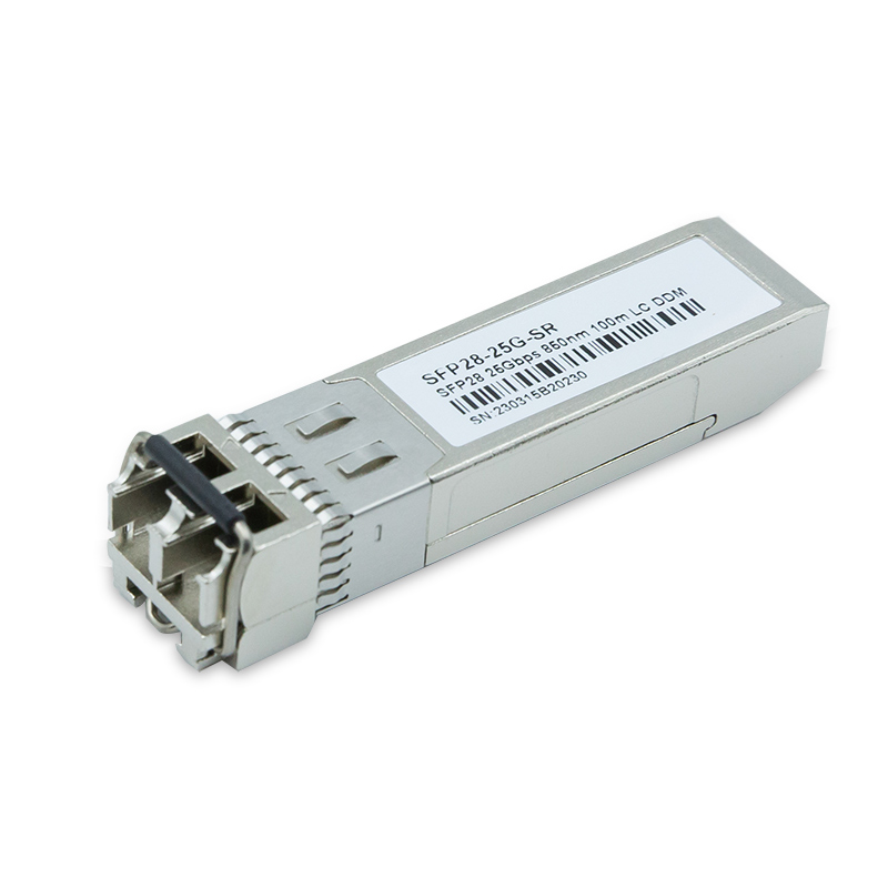
25Gbps 850nm SFP28 Transceiver
XTSL28S8501DC
25 Gbps 850nm SFP28 Transceiver
Features
nHot-pluggable SFP+ footprint
nSupport 25.78 Gbps bit rate
n850 nm VCSEL laser and PIN photo-detector
nMaximum link length of 100m on OM4 MMF
nPower Dissipation <1W
nSingle +3.3V power supply
nLC duplex connector
Operating Case temperature range 0°C to 70°C
nRoHS-6 compliant
nCompliant with SFF-8431
nCompliant with SFF-8472
nCompliant with IEEE 802 . 3by 25 GBASE-SR
Applications
n25 GBASE-SR Ethernet
nOther Optical Links
Ordering information
Part No. | Data Rate | Laser | Temp. | Optical Interface | DDMI |
XTSL28S8501 DC | 25.78Gbps | VCSEL | 0°C to 70°C | Duplex LC | YES |
Description
XTSL28S8501DC transceivers is designed for using in 25Gb/s data rate over multimode fiber. The transceiver is compliant with SFF-8431, and the mechanical SFP28 plug is compatible with SFF-8432. Digital diagnostics functions are available via a 2-wire serial interface, as specified in SFF-8472.
Absolute Maximum Ratings
Parameter | Symbol | Min. | Typical | Max. | Unit | Note |
Power Supply Voltage | VCC | 0 | 3.6 | V | ||
Storage Temperature | Ts | -40 | +85 | 。C | ||
Relative Humidity | RH | 5 | 85 | % | Non-condensing | |
Operating Case Temperature | Tc | 0 | +70 | °C |
Electrical Characteristics
Parameter | Symbol | Min. | Typical | Max. | Unit | Note |
Power Supply Voltage | VCC | 3.135 | 3.3 | 3.465 | V | |
Power Dissipation | PD | 1 | W | |||
Power Supply Current | Icc | 300 | mA | |||
Data Rate | 25.78 | Gb ps | ||||
Clock Rate-I2C | 400 | kHz | ||||
Transmitter | ||||||
Input Differential impedance | Z IN | 100 | ohm | |||
Differential data input swing | VIN | 250 | 900 | mV | ||
Transmit Disable Voltage | V DIS | 2 | VCC+0.3 | V | ||
Transmit Enable Voltage | VEN | 0 | 0.8 | V | ||
Transmit Fault Assert Voltage | 2 | VCC+0.3 | V | |||
Transmit Fault De-Assert Voltage | 0 | 0.8 | V | |||
Receiver | ||||||
Output Differential impedance | Zout | 100 | ohm | |||
Differential data Output Swing | Vout | 300 | 850 | mV | ||
Rx_LOS Output Voltage-High | 2 | VCC+0.3 | V | |||
Rx_LOS Output Voltage-Low | 0 | 0.8 | V | |||
Optical Parameters
Parameter | Symbol | Min. | Typical | Max. | Unit | Note |
Power budget (for max TEDC) | 8.2 | dB | ||||
Data Rate | 25.78 | Gb ps | ||||
Transmitter | ||||||
Center Wavelength | λ | 840 | 850 | 860 | nm | |
RMS spectral width | ΔλRMS | 0.6 | nm | |||
Average Optical Power | PAVG | -8.4 | 2.4 | dBm | ||
Laser Off Power | POFF | -30 | dBm | |||
Extinction Ratio | ER | 2 | 4 | dB | ||
Transmitter and dispersion eye closure | TDEC | 4.3 | dB | |||
Relative Intensity Noise | RIN | -128 | dB/ Hz | |||
Receiver | ||||||
Center Wavelength | λ | 840 | 850 | 860 | nm | |
Receiver Sensitivity (OMA) | RSENSE1 | -10 | dBm | 1 | ||
Maximum Input Power | Pmax | 3.4 | dBm | |||
Los Assert | LOSA | -30 | dBm | |||
Los Dessert | LOSD | -12 | dBm | |||
Los Hysteresis | LOSH | 0.5 | dB | |||
Receiver Reflectance | RREFL | -12 | dB | |||
Note1:Sensitivity for 25.78 Gb/s PRBS31 and BER better than or equal to 5 E-5 .
General Specifications
Parameter | Symbol | Min. | Typical | Max. | Unit | Note | |
Bit Rate | BR | 25.78 | Gb ps | ||||
Bit Error Ratio | BER | 5E-5 | PRBS31 | ||||
Maximum Supported Distances | |||||||
Fiber Type | Bandwidth (850nm) | ||||||
50um | 2000MHz* km | 70 | m | OM3 | |||
50um | 4700MHz* km | 100 | m | OM4 | |||
Digital Diagnostic Functions
XTSL28S8501DC transceivers can be used in host systems that require either internally or externally calibrated digital diagnostics.
Parameter | Symbol | Min. | Typical | Max. | Unit | Note |
Temperature monitor absolute error | -3 | 3 | 。C | |||
Laser power monitor absolute error | -3 | 3 | dB | |||
RX power monitor absolute error | -3 | 3 | dB | |||
Supply voltage monitor absolute error | -100 | 100 | mV | |||
Bias current monitor | -10% | 10% | mA |
Pin Assignment:


Pin Descriptions
PIN | Symbol | Name / Description | Note |
1 | VEET | Transmitter Ground (Common with Receiver Ground) | 1 |
2 | TX_Fault | Transmitter Fault | 2 |
3 | TX_Dis | Transmitter Disable | 3 |
4 | SDA | 2-Wire Serial Interface Data Line | 4 |
5 | SCL | 2-Wire Serial Interface Clock | 4 |
6 | MOD_ ABS | Module Definition, Grounded in the module | 4 |
7 | RS0 | Receiver Rate Select ( Low= ≤ 10.3 Gbps, High=25.78 Gbps) | 5 |
8 | RX_ LOS | Receiver Loss of Signal Indication | 6 |
9 | RS1 | Transmitter Rate Select ( Low= ≤ 10.3 Gbps, High=25.78 Gbps) | 5 |
10 | VEER | Receiver Ground (Common with Transmitter Ground) | 1 |
11 | VEER | Receiver Ground (Common with Transmitter Ground) | 1 |
12 | RD- | Receiver Inverted Data Output | 7 |
13 | RD+ | Receiver Data Output | 7 |
14 | VEER | Receiver Ground (Common with Transmitter Ground) | 1 |
15 | VCCR | Receiver Power | 8 |
16 | VCCT | Transmitter Power | 8 |
17 | VEET | Transmitter Ground (Common with Receiver Ground) | 1 |
18 | TD+ | Transmitter Non-Inverted Data Input | 7 |
19 | TD- | Transmitter Inverted Data Input | 7 |
20 | VEET | Transmitter Ground (Common with Receiver Ground) | 1 |
Note1: Module ground pins GND are isolated from the module case.
Note2: The Tx_Fault output is an open collector/drain output, which should be pulled up with a 4.7k to 10 k ohms resistor on the host
board. Pull up voltage should be between 2 .0V to Vcc+0.3V . A high output indicates a transmitter fault caused by either the TX bias
current or the TX output power exceeding the preset alarm thresholds. A low output indicates normal operation. In the low state,
the output is pulled to<0 .8V
Note3 : Laser output disabled on TDIS >2 .0V or open, enabled on TDIS <0.8V .
Note4: Shall be pulled up with 4.7K-10 Kohms to a voltage between 3. 15V and 3.45V on the host board.
Note5 : Rate select can also be set through the 2- wire bus in accordance with SFF-84 72 . Rx Rate select at Bit3 , Byte 110 ,
Address A2h. Tx Rate Select is set at Bit 3, Byte 118 , Address A2h.
Note6 : LOS is open collector output. Should be pulled up with 4 .7-10 k ohms on host board to a voltage between 2 .0V and 3.6V
Logic 0 indicates normal operation; logic 1 indicates loss of signal.
Note7 : They areAC-coupled, differential lines with 100 Ω differential termination inside the module.
Note8 : VccR and VccT are the receiver and transmitter power supplies. They are defined as 3.3 V ± 5 % at the SFP+ connector pin.
Mechanical Dimensions

Revision History
Revision | Initiated | Reviewed | Approved | DCN | Release Date |
V1.0 | Feynman | XX | XX | Released. | July 16, 2022 |
Important Notice
Performance figures, data and any illustrative material provided in this data sheet are typical and must be specifically confirmed in writing by Zkosemi before they become applicable to any particular order or contract. In accordance with the Zkosemi policy of continuous improvement specifications may change without notice . The publication of information in this data sheet does not imply freedom from patent or other protective rights of Zkosemi or others. Further details are available from any Zkosemi sales representative .