

Product type
 Contact Information
+86 755 89660635
+86 189 2461 3736

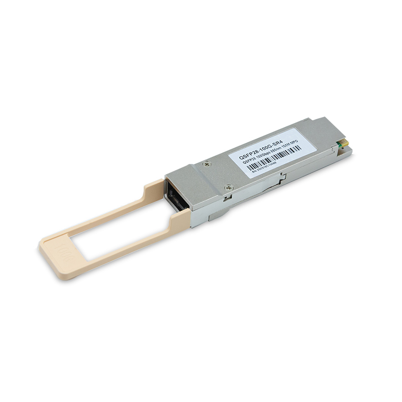
100G QSFP28 SR4 Optical Transceiver
XTQM1HS8501DC
100Gbps 850nm QSFP28 Transceiver
Features
n Hot-pluggable QSFP28 footprint
n Support 103.1Gbps aggregate bit rate
n 4x25Gbps 850nm VCSEL transmitter
n 4x25Gpbs electrical interface
n Maximum link length of 100m on OM4 MMF
n Power Dissipation <2.5W
n Single +3.3V power supply
n Single MPO12 receptacle
n Operating Case temperature range 0°C to 70°C
n RoHS-6 compliant
n Compliant with SFF-8679
n Compliant with SFF-8636
n Compliant with IEEE 802.3bm 100GBASE-SR4
Applications
n 100GBASE-SR4 Ethernet
n Date Center
n Other Optical Links
Ordering information
Part No. | Data Rate | Laser | Temp. | Optical Interface | DDMI |
XTQM1HS8501DC | 103.1Gbps | VCSEL | 0°C to 70°C | MPO12 | YES |
Description
XTQM1HS8501DC transceivers is designed for using in 100Gb/s data rate over multimode fiber. The transceiver is compliant with SFF-8679, and the mechanical QSFP28 plug is compatible with SFF-8661. Digital diagnostics functions are available via a 2-wire serial interface, as specified in SFF-8636.
Absolute Maximum Ratings
Parameter | Symbol | Min. | Typical | Max. | Unit | Note |
Power Supply Voltage | VCC | 0 | 3.6 | V | ||
Storage Temperature | Ts | -40 | +85 | 。C | ||
Relative Humidity | RH | 5 | 85 | % | Non-condensing | |
Case Operating Temperature | Tc | 0 | +70 | °C |
Electrical Characteristics
Parameter | Symbol | Min. | Typical | Max. | Unit | Note |
Power Supply Voltage | VCC | 3.135 | 3.3 | 3.465 | V | |
Power Dissipation | PD | 2.5 | W | |||
Power Supply Current | Icc | 800 | mA | |||
Aggregate Data Rate | 103.1 | Gbps | ||||
Signaling rate per lane | 25.78 | Gbps | ||||
Clock Rate-I2C | 400 | kHz | ||||
Transmitter | ||||||
Input Differential impedance | ZIN | 100 | ohm | |||
Differential data input swing | VIN | 180 | 900 | mV | ||
Single-ended voltage tolerance | -0.3 | 3.3 | V | |||
Receiver | ||||||
Output Differential impedance | Zout | 100 | ohm | |||
Differential data Output Swing | Vout | 300 | 850 | mV | ||
Optical Parameters
Parameter | Symbol | Min. | Typical | Max. | Unit | Note |
Power budget (for max TEDC) | 8.2 | dB | ||||
Aggregate Data Rate | 103.1 | Gbps | ||||
Signaling rate per lane | 25.78 | Gbps | ||||
Transmitter | ||||||
Center Wavelength | λ | 840 | 850 | 860 | nm | |
RMS spectral width | ΔλRMS | 0.6 | nm | |||
Average Optical Power | PAVG | -8.4 | 2.4 | dBm | ||
Laser Off Power | POFF | -30 | dBm | |||
Extinction Ratio | ER | 2 | 4 | dB | ||
Transmitter and dispersion eye closure | TDEC | 4.3 | dB | |||
Optical Return Loss Tolerance | ORL | 12 | dB | |||
Receiver | ||||||
Center Wavelength | λ | 840 | 850 | 860 | nm | |
Receiver Sensitivity (OMA) | RSENSE1 | -10 | dBm | 1 | ||
Stressed Receiver Sensitivity (OMA) | SRS | -5.2 | dBm | |||
Maximum Input Power | Pmax | 3.4 | dBm | |||
Los Assert | LOSA | -30 | dBm | |||
Los Dessert | LOSD | -11 | dBm | |||
Los Hysteresis | LOSH | 0.5 | dB | |||
Receiver Reflectance | RREFL | -12 | dB |
Note1:Sensitivity for 25.78Gb/s PRBS31 and BER better than or equal to 5E-5.
General Specifications
Parameter | Symbol | Min. | Typical | Max. | Unit | Note | |
Aggregate Data Rate | 103.1 | Gbps | |||||
Signaling rate per lane | 25.78 | Gbps | |||||
Bit Error Ratio (pre-FEC) | BER | 5E-5 | PRBS31 | ||||
Maximum Supported Distances | |||||||
Fiber Type | Bandwidth (850nm) | ||||||
50um | 2000MHz*km | 70 | m | OM3 | |||
50um | 4700MHz*km | 100 | m | OM4 | |||
Digital Diagnostic Functions
XTQM1HS8501DC transceivers can be used in host systems that require either internally or externally calibrated digital diagnostics.
Parameter | Symbol | Min. | Typical | Max. | Unit | Note |
Temperature monitor absolute error | -3 | 3 | 。C | |||
Laser power monitor absolute error | -3 | 3 | dB | |||
RX power monitor absolute error | -3 | 3 | dB | |||
Supply voltage monitor absolute error | -100 | 100 | mV | |||
Bias current monitor | -10% | 10% | mA |
Pin Assignment:

Pin Descriptions
PIN | Symbol | Name / Description | Note |
1 | GND | Ground | 1 |
2 | Tx2n | Transmitter Inverted Data Input | |
3 | Tx2p | Transmitter Non-Inverted Data Input | |
4 | GND | Ground | 1 |
5 | Tx4n | Transmitter Inverted Data Input | |
6 | Tx4p | Transmitter Non-Inverted Data Input | |
7 | GND | Ground | 1 |
8 | ModSelL | Module Select | 2 |
9 | ResetL | Module Reset | |
10 | Vcc Rx | 3.3V Power Supply Receiver | |
11 | SCL | 2-wire serial interface clock | 3 |
12 | SDA | 2-wire serial interface data | 3 |
13 | GND | Ground | 1 |
14 | Rx3p | Receiver Non-Inverted Data Output | |
15 | Rx3n | Receiver Inverted Data Output | |
16 | GND | Ground | 1 |
17 | Rx1p | Receiver Non-Inverted Data Output | |
18 | Rx1n | Receiver Inverted Data Output | |
19 | GND | Ground | 1 |
20 | GND | Ground | 1 |
21 | Rx2n | Receiver Inverted Data Output | |
22 | Rx2p | Receiver Non-Inverted Data Output | |
23 | GND | Ground | 1 |
24 | Rx4n | Receiver Inverted Data Output | |
25 | Rx4p | Receiver Non-Inverted Data Output | |
26 | GND | Ground | 1 |
27 | ModPrsL | Module Present | 3 |
28 | IntL | Interrupt | 3 |
29 | Vcc Tx | 3.3V power supply transmitter | |
30 | Vcc1 | 3.3V power supply | |
31 | LPMode | Low Power Mode | |
32 | GND | Ground | 1 |
33 | Tx3p | Transmitter Non-Inverted Data Input | |
34 | Tx3n | Transmitter Inverted Data Input | |
35 | GND | Ground | 1 |
36 | Tx1p | Transmitter Non-Inverted Data Input | |
37 | Tx1n | Transmitter Inverted Data Input | |
38 | GND | Ground | 1 |
Note1: Module ground pins GND are isolated from the module case.
Note2: ModSelL is an input signal. When held low by the host, the module responds to two-wire serial communication commands. The ModSelL signal allows the use of multiple modules on a single two-wire interface. When ModSelL is high, the module shall not respond to or acknowledge any two-wire interface communication from the host.
Note3: Shall be pulled up with 4.7K-10Kohms to a voltage between 3.15V and 3.45V on the host board.
Mechanical Dimensions

Revision History
Revision | Initiated | Reviewed | Approved | DCN | Release Date |
V1.0 | Feynman | XX | XX | Released. | July 16, 2022 |
Important Notice
Performance figures, data and any illustrative material provided in this data sheet are typical and must be specifically confirmed in writing by Zkosemi before they become applicable to any particular order or contract. In accordance with the Zkosemi policy of continuous improvement specifications may change without notice. The publication of information in this data sheet does not imply freedom from patent or other protective rights of Zkosemi or others. Further details are available from any Zkosemi sales representative.