

Product type
 Contact Information
+86 755 89660635
+86 189 2461 3736

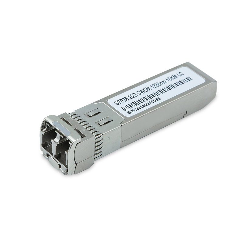
25GBASE SFP28 CWDM 1270nm~1610nm 10km LC DDM SMF Optical Transceiver Module
ZK-SFP28-25G-CWDM10
25Gbps SFP28 CWDM 10km SMF Transceiver
Features
n Compatible with CPRI option10 24.33Gbps and 25.78Gbp
n Up to 10km on 9/125µm SMF
n Electrical interface specifications per SFF-8431,SFF-8472
n Duplex LC connector
n Single +3.3V DC power supply
n Hot-pluggable SFP footprint
n Class 1 laser safety certified
n Operating temperature Options
Commercial:0~+70℃
Industrial: -40 to +85℃
n RoHS Compliant
Applications
n 25GBASE-LR
Ordering information
Part No. | Data Rate | Transmitter | Reach | Optical Interface | DDMI |
ZK-SFP28-25G-CWDM-27 | 25.78Gbps | 1270 | 10KM | LC | YES |
ZK-SFP28-25G-CWDM-29 | 25.78Gbps | 1290 | 10KM | LC | YES |
ZK-SFP28-25G-CWDM-31 | 25.78Gbps | 1310 | 10KM | LC | YES |
ZK-SFP28-25G-CWDM-33 | 25.78Gbps | 1330 | 10KM | LC | YES |
ZK-SFP28-25G-CWDM-35 | 25.78Gbps | 1350 | 10KM | LC | YES |
ZK-SFP28-25G-CWDM-37 | 25.78Gbps | 1370 | 10KM | LC | YES |
Description
ZK-SFP28-25G-CWDM-27 25G SFP28 transceivers are designed for 24.33Gbps and 25.78Gbps data rate over SMF and support up to 10km link length. They are compliant to IEEE802.3ba, SFF-8402, SFF-8432. Digital diagnostic monitoring interface compliant to SFF-8472 is available via an I2C interface.
Pin Description
Pin | Name | Function/Description | Engagement order (Insertion) | Notes |
1 | VeeT | Transmitter Ground | 1 | - |
2 | TX Fault | Transmitter Fault Indication | 3 | 1 |
3 | TX Disable | Transmitter Disable-Module disables on high or open | 3 | 2 |
4 | SDA | 2-wire Serial Interface Data Line (Same as MOD-DEF2 as defined in the INF-8074i) | 3 | 3 |
5 | SCL | 2-wire Serial Interface Clock (Same as MOD-DEF1 as defined in the INF-8074i) | 3 | 3 |
6 | MOD-ABS | Module Absent, connected to VeeT or VeeR in the module | 3 | 3 |
7 | RS0 | Receiver Rate Select | 3 | - |
8 | LOS | Loss of Signal | 3 | 4 |
9 | RS1 | Transmitter Rate Select (not used) | 1 | - |
10 | VeeR | Receiver Ground | 1 | - |
11 | Veer | Receiver Ground | 1 | - |
12 | RD- | Inverse Received Data out | 3 | 5 |
13 | RD+ | Received Data out | 3 | 5 |
14 | VeeR | Receiver Ground | 1 | - |
15 | VccR | Receiver Power - +3.3V±5% | 2 | 6 |
16 | VccT | Transmitter Power - +3.3 V±5% | 2 | 6 |
17 | VeeT | Transmitter Ground | 1 | - |
18 | TD+ | Transmitter Data In | 3 | 7 |
19 | TD- | Inverse Transmitter Data In | 3 | 7 |
20 | VeeT | Transmitter Ground | 1 | - |
Notes:
1. TX Fault is open collector/drain output which should be pulled up externally with a 4.7KΩ-10KΩ resistor on the host board to supply < VccT +0.3V or VccR + 0.3V. When high, this output indicates a laser fault of some kind. Low indicates normal operation. In the low state, the output will be pulled to <0.8V.
2. TX Disable input is used to shut down the laser output per the state table below. It is pulled up within the module with a 4.7KΩ-10KΩ resistor.
Low (0 – 0.8V): | Transmitter on |
Between (0.8V and 2V): | Undefined |
High (2.0 – VccT): | Transmitter Disabled |
Open : | Transmitter Disabled |
3. Mod-Def 0, 1, 2. These are the module definition pins. They should be pulled up with a 4.7KΩ-10KΩ resistor on the host board to supply less than VccT+0.3V or VccR+0.3V.
Mod-Def 0 is grounded by the module to indicate that the module is present.
Mod-Def 1 is clock line of two wire serial interface for optional serial ID.
Mod-Def 2 is data line of two wire serial interface for optional serial ID.
4. LOS (Loss of signal) is an open collector/drain output which should be pulled up externally with a 4.7KΩ-10KΩ resistor on the host board to supply <VccT+0.3V or VccR+0.3V. When high, this output indicates the received optical power is below the worst case receiver sensitivity (as defined by the standard in use). Low indicates normal operation. In the low state, the output will be pulled to <0.8V.
5. RD-/+: These are the differential receiver outputs. They are AC coupled 100Ω differential lines which should be terminated with 100Ω differential at the user SERDES. The AC coupling is done inside the module and thus not required on the host board.
6. VccR and VccT are the receiver and transmitter power supplies. They are defined as 3.3V±5% at the SFP connector pin. The in-rush current will typically be no more than 30mA above steady state supply current after 500ns.
7. TD-/+: These are the differential transmitter inputs. They are AC coupled differential lines with 100Ω differential termination inside the module. The AC coupling is done inside the module and is thus not required on host board.

Absolute Maximum Ratings
Stresses in excess of the absolute maximum ratings can cause permanent damage to the device. These are absolute stress ratings only. Functional operation of the device is not implied at these or any other conditions in excess of those given in the operational sections of the data sheet. Exposure to absolute maximum ratings for extended periods can adversely affect device reliability
Parameter | Symbol | Minimum | Maximum | Unit |
Storage Temperature | TS | -40 | 85 | oC |
Relative Humidity | RH | 5 | 95 | % |
Supply Voltage | VCC | -0.5 | 4.0 | V |
Recommended Operating Conditions
Parameter | Symbol | Min | Typ | Max | Unit |
Operating Case Temperature | TC | -40 | 25 | 85 | oC |
Supply Voltage | VCC | 3.135 | 3.3 | 3.465 | V |
Total power Consumption | Pd | 1.5 | W | ||
Data Rate | - | 25.78125 | Gbps |
Transceiver Electrical Characteristics
Parameter | Symbol | Minimum | Typical | Maximum | Unit | Notes |
Module Supply Current | Icc | - | - | 450 | mA | - |
Transmitter Differential Input Voltage (TD +/-) | - | 300 | - | 1100 | mVP-P | 1 |
Receiver Differential Output Voltage (RD +/-) | - | 500 | - | 800 | mVP-P | 2 |
Low speed output: Transmitter Fault(TX_FAULT) / Loss of Signal (LOS) | VOH | 2.0 | - | Vcc | V | 3 |
VOL | 0 | - | 0.8 | V | - | |
Low speed iutput: Transmitter Disable (TX_DISABLE), MOD_DEF 1, MOD_DEF 2 | VIH | 2.0 | - | Vcc | V | 4 |
VIL | 0 | - | 0.8 | V | - |
Notes:
1. Internally AC coupled and terminated to 100Ω differential load.
2. Internally AC coupled, but requires a 100Ω differential termination or internal to Serializer/Deserializer.
3. Pulled up externally with a 4.7KΩ-10KΩ resistor on the host board to VCCT,R.
4. Mod_Def1 and Mod_Def2 must be pulled up externally with a 4.7KΩ-10KΩ resistor on the host board to VCCT,R.
Transmitter Optical Characteristics
Parameter | Symbol | Minimum | Typical | Maximum | Unit | Notes |
Launch Optical Power | Po | 1 | - | 7 | dBm | - |
Center Wavelength Range | λc | 1260 | 1380 | nm | - | |
Extinction Ratio | ER | 3.5 | - | - | dB | - |
Side Mode Suppression Rati | SMSR | 30 | nm | |||
Spectral Width (-20dB) | Δλ | - | - | 1 | nm | |
Optical Rise/Fall Time | Trise/Tfall | - | - | 50 | ps | - |
Pout @TX-Disable Asserted | Poff | - | - | -30 | dBm | - |
Eye Diagram | {0.31, 0.4, 0.45, 0.34, 0.38, 0.4} | |||||
Receiver Optical Characteristics
Parameter | Symbol | Minimum | Typical | Maximum | Unit | Notes |
Wavelength Range | λc | 1260 | 1380 | nm | - | |
Receiver Sensitivity | Sen | - | - | -13.5 | dBm | - |
Receiver Overload | POL | 2.5 | - | - | dBm | - |
LOS De-Assert | LOSD | - | -17 | dBm | - | |
LOS Assert | LOSA | -30 | - | - | dBm | - |
LOS Hysteresis | - | 0.5 | - | - | dB | - |
Digital Diagnostic Memory Map
The transceivers provide serial ID memory contents and diagnostic information about the present
operating conditions by the 2-wire serial interface (SCL, SDA).The diagnostic information with internal calibration or external calibration all are implemented, including received power monitoring, transmitted power monitoring, bias current monitoring, supply voltage monitoring and temperature monitoring. The digital diagnostic memory map specific data field defines as following.

Host Board Power Supply Filter Network

Mechanical specifications

Important Notice
Performance figures, data and any illustrative material provided in this data sheet are typical and must be specifically confirmed in writing by Zkosemi before they become applicable to any particular order or contract. In accordance with the Zkosemi policy of continuous improvement specifications may change without notice. The publication of information in this data sheet does not imply freedom from patent or other protective rights of Zkosemi or others. Further details are available from any Zkosemi sales representative.