

Product type
 Contact Information
+86 755 89660635
+86 189 2461 3736

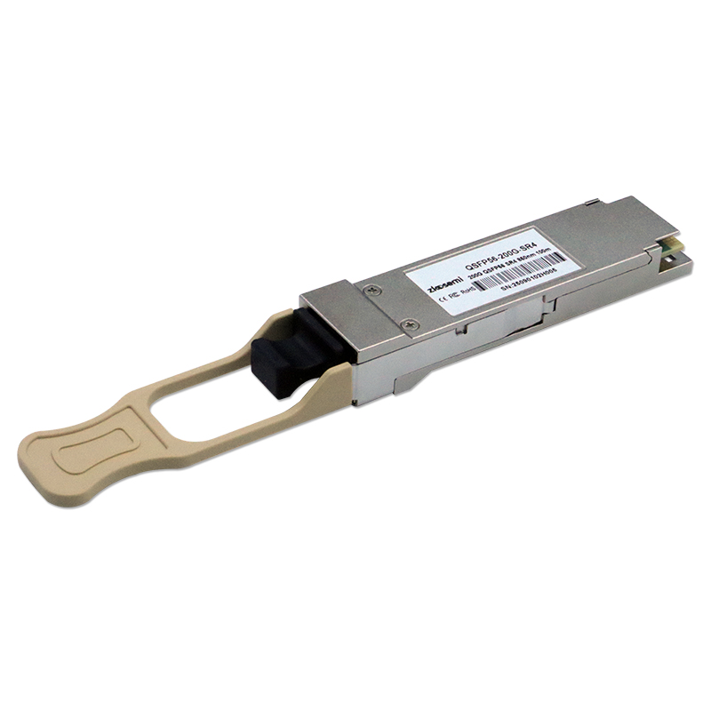
200GBASE SR4 QSFP56 850nm 100m MPO-12/UPC DDM MMF Optical Transceiver Module
ZK-QSFP56-200G-SR4
200Gbps QSFP5 SR4 850nm 100m Transceiver
Features
n Hot-pluggable QSFP56 form factor
n Data Rate up to 53.125 Gb/s PAM4 per lane
n 4×53Gbps PAM4 transmitter and PAM4 receiver
n 4 channels 850nm VCSELlaser array and 4 channels PIN photo-detector array
n Maximum link length of 70m on OM3 MMF and 100m on OM4MMF
n Digital diagnostics functions are available via the 12C interface
n Single 3.3V Power Supply
n MPO-12 PC connector
n Operating Case Temperature:0℃~+70℃
n RoHS compliant
Applications
n 200GBASE-SR4 Ethernet
Description
ZK-QSFP56-200G-SR4 is a 4-Channel,Pluggable,Fiber-OpticQSFP56 for 200Gbps SR Applications.It is ahigh performance module for short-range data communication and interconnect applications which operate at 53.125Gbps per lane up to 70m using OM3fiber and 100m using OM4 fiber.The optical interface uses MPO receptacles.This module is designed to operate over multimode fiber systems using a nominal wavelength of 850nm. The electrical interface uses a 38 contact edge type connector.
Absolute Maximum Ratings
These values represent the damage threshold of the module.Stress in excess of any of the individual Absolute Maximum Ratings can cause immediate catastrophic damage to the module even if all other parameters are within Recommended Operating Conditions.
Parameters | Symbol | Min. | Max. | Unit |
Power Supply Voltage | VCC | -0.5 | +3.6 | V |
Storage Temperature | Tc | -40 | +85 | ℃ |
Relative Humidity | RH | 0 | 85 | % |
Recommended Operating Environment
Recommended Operating Environment specifies parameters for which the electrical and optical characteristics hold unless otherwise noted.
Parameter | Symbol | Min. | Typical | Max. | Unit |
Power Supply Voltage | VCC | 3.15 | 3.30 | 3.45 | V |
Operating Case Temperature | Tca | 0 | 70 | C |
Electrical Characteristics
The following electrical characteristics are defined over the Recommended Operating Environment unless otherwise specified.
Parameter | Symbol | Min. | Typical | Max. | Unit | Note |
Data Rate per lane | DR | 53.125 | Gbps | |||
Transmitter | ||||||
Single Ended Output Voltage Tolerance | -0.3 | 4.0 | V | |||
Common mode voltage tolerance | 15 | - | mV | |||
Input differential impedance | Rin | 100 | Ω | |||
Differential Input Voltage swing | Vin | 300 | 1 | 1100 | mV | |
Tx Fault | VoL | -0.3 | 0.4 | V | At 0.7mA | |
Receiver | ||||||
Single Ended Output Voltage Tolerance | -0.3 | 4.0 | V | |||
Differential Output Swing | Vout | 300 | - | 900 | mV | |
Output differential impedance | Rout | 100 | Ω | |||
Optical Parameters
The following optical characteristics are defined over the Recommended Operating Environment unless otherwise specified.
Parameter | Symbol | Min. | Typical | Max. | Unit | Note |
Transmitter | ||||||
Center Wavelength | λ | 820 | 850 | 880 | nm | |
RMS spectral width | Pm | - | - | 0.6 | nm | 1 |
Average Optical Power | Po | -6.5 | - | 4 | dBm | 2 |
Extinction Ratio | ER | 3.0 | - | - | dBm | |
Optical Modulation Amplitude | OMA | -4.5 | 3 | dB | ||
Transmitter and Dispersion Eye Closure | TDECQ | 4.5 | dB | |||
Optical Return Loss Tolerance | ORL | - | - | 12 | dB | |
Receiver | ||||||
Center Wavelength | λ | 820 | 880 | nm | ||
Average Receive power,each lane | -8.4 | 4 | dBm | |||
Receive power(OMAouter),each lane | 4 | dBm | ||||
Receiver Sensitivity(OMAout) | Psens | - | - | -6.5 | dBm | 3 |
LOS Asserted | Lsa | -30 | - | - | dBm | |
LOS De-Asserted | Lda | - | - | -10 | dBm | |
LOS Hysteresis | Lh | 0.5 | - | dB | ||
Note:
1. Trade-offs are available between spectral width,center wavelength and minimum OMA.
2. The optica power is launched into MMF
3. BER=2.4E-4;PRBS31Q@26.5625GBd.Pre-FEC
Pin Assignment
Pin Descriptions
PIN | Symbol | Name / Description |
1 | GND | Ground |
2 | Tx2n | Transmitter Inverted Data Input |
3 | Tx2p | Transmitter Non-Inverted Data Input |
4 | GND | Ground |
5 | Tx4n | Transmitter Inverted Data Input |
6 | Tx4p | Transmitter Non-Inverted Data Input |
7 | GND | Ground |
8 | ModSelL | Module Select |
9 | ResetL | Module Reset |
10 | Vcc Rx | 3.3V Power Supply Receiver |
11 | SCL | 2-wire serial interface clock |
12 | SDA | 2-wire serial interface data |
13 | GND | Ground |
14 | Rx3p | Receiver Non-Inverted Data Output |
15 | Rx3n | Receiver Inverted Data Output |
16 | GND | Ground |
17 | Rx1p | Receiver Non-Inverted Data Output |
18 | Rx1n | Receiver Inverted Data Output |
19 | GND | Ground |
20 | GND | Ground |
21 | Rx2n | Receiver Inverted Data Output |
22 | Rx2p | Receiver Non-Inverted Data Output |
23 | GND | Ground |
24 | Rx4n | Receiver Inverted Data Output |
25 | Rx4p | Receiver Non-Inverted Data Output |
26 | GND | Ground |
27 | ModPrsL | Module Present |
28 | IntL | Interrupt |
29 | Vcc Tx | 3.3V power supply transmitter |
30 | Vcc1 | 3.3V power supply |
31 | LPMode | Low Power Mode |
32 | GND | Ground |
33 | Tx3p | Transmitter Non-Inverted Data Input |
34 | Tx3n | Transmitter Inverted Data Input |
35 | GND | Ground |
36 | Tx1p | Transmitter Non-Inverted Data Input |
37 | Tx1n | Transmitter Inverted Data Input |
38 | GND | Ground |
Mechanical

Important Notice
Performance figures, data and any illustrative material provided in this data sheet are typical and must be specifically confirmed in writing by Zkosemi before they become applicable to any particular order or contract. In accordance with the Zkosemi policy of continuous improvement specifications may change without notice. The publication of information in this data sheet does not imply freedom from patent or other protective rights of Zkosemi or others. Further details are available from any Zkosemi sales representative.