

Product type
 Contact Information
+86 755 89660635
+86 189 2461 3736

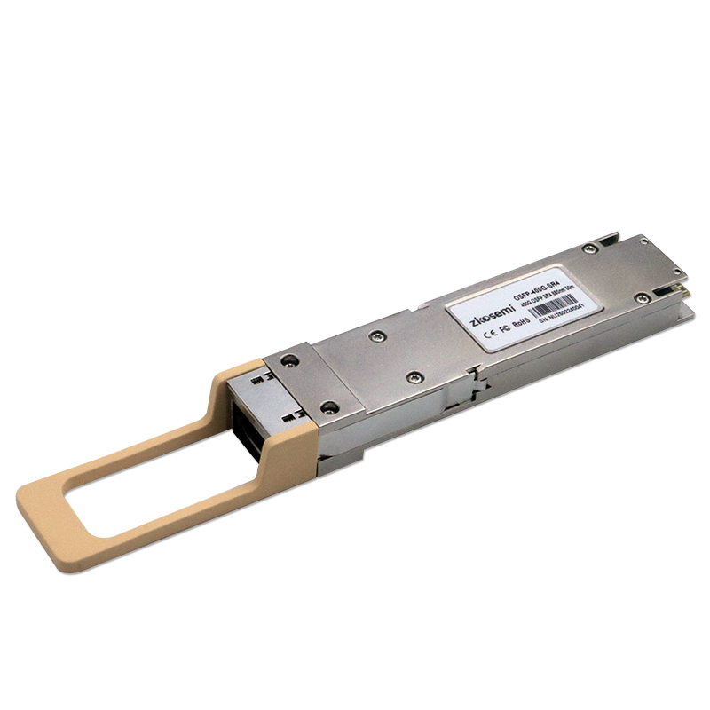
400GBASE SR4 OSFP 850nm 50m MPO-12/APC DDM MMF Optical Transceiver Module
ZK-OSFP-400G-SR4
400Gbps OSFP SR4 850nm 50m MMF Transceiver
Features
n Supports 425Gbps
n Single 3.3V Power Supply
n Power dissipation:
Commercial version <8W
n 4x53.125GBd (PAM4) Electrical Interface
n MPO-12 Connector APC
n Up to 50m over OM4 and 30m over OM3
n Case Temperature Range: 0°C to 70°C
n VCSEL Transmitter
n PIN and TIA Array on the Receiver Side
n I2C Interface with Integrated Digital Diagnostic Monitoring
n Safety Certification: TUV/UL/FDA*1
n RoHS Compliant
n OSFP MSA Compliant
Applications
n 400GBASE-VR4
Description
OSFP 400G SR4 transceiver module is designed for use in 400G Ethernet links up to 50m over
OM4 and 30m over OM3 multi-mode fiber. The module has 4 independent electrical input/output channels
operating at 106.25Gbps per channel. This transceiver consists a transmitter/receiver unit operating on 850nm
wavelengths. The transmitter path of the module incorporates a PAM4 re-timer ASIC integrated with a
4-channel modulators driver, 4 externally modulated lasers. On the receiver path, there are 4 photodiodes and
one 4-channel linear TIA arrays, along with the PAM4 re-timer. The electrical interface of the module is
compliant with the 400GAUI-4 interface as defined by IEEE 802.3ck.

Absolute Maximum Ratings
Parameter | Symbol | Min | Typ. | Max | Unit |
Storage Temperature | Ts | -40 | 85 | °C | |
Power Supply Voltage | Vcc | -0.5 | 3.3 | 3.6 | V |
Relative Humidity (non-Condensing) | RH | 5 | 85 | % |
Recommended Operating Conditions
Parameter | Symbol | Min. | Typ. | Max. | Unit | Note |
Operating Case Temperature | Tc | 0 | 70 | °C | ||
Power Supply Voltage | Vcc | 3.135 | 3.3 | 3.465 | V | |
Power Supply Noise | 50 | mVpp | ||||
Receiver Differential Data Output Load | 100 | Ohm | ||||
Fiber Length (OM3) | OM3 | 30 | m | |||
Fiber Length (OM4) | OM4 | 50 | m |
Note:
1. Power Supply specifications, Instantaneous, sustained and steady state current compliant with QSFP112 MSA Power Classification.
Optical Characteristics
Parameter | Symbol | Min. | Typ. | Max. | Unit | Note |
Transmitter | ||||||
Signaling Rate, each Lane | DR | 53.125±100ppm | GBd | |||
Modulation Format | PAM4 | |||||
Center Wavelength | λ | 842 | 948 | nm | ||
RMS Spectral Width | RMS | 0.6 | nm | |||
Average Launch Power, each Lane | Pavg | -4.6 | 4 | dBm | ||
Outer Optical Modulation Amplitude (OMAouter), each Lane (max) | POMA | 3.5 | dBm | |||
Outer Optical Modulation Amplitude(OMAouter), each Lane (min) for max (TECQ, TDECQ) ≤1.8dB | POMA | -2.6 | dBm | |||
Outer Optical Modulation Amplitude(OMAouter), each Lane (min) for 1.8<max (TECQ, TDECQ) ≤4.4dB | POMA | -4.4+max (TECQ,TDECQ) | dBm | |||
TDECQ (PAM4), Per Lane | TDECQ | 4.4 | dB | |||
Overshoot/Undershoot | 29 | % | ||||
Transmitter Power Excursion, each Lane | 2.3 | dBm | ||||
Extinction Ratio, each Lane | ER | 2.5 | dB | |||
Transmitter Transition Time, each Lane | 17 | ps | ||||
Average Launch Power of OFF Transmitter, each Lane | Poff | -30 | dBm | |||
RIN12OMA | RIN12OMA | -132 | dB/Hz | |||
Optical Return Loss Tolerance | ORL | 12 | dB | |||
Encircled Flux | EF | ≥86% at 19 mm ≤30% at 4.5 mm | ||||
Receiver | ||||||
Signaling Rate, each Lane | 53.125± 100ppm | GBd | ||||
Modulation Format | PAM4 | |||||
Center Wavelength | λ | 842 | 948 | nm | ||
Damage Threshold | 5 | dBm | ||||
Average Receiver Power, each Lane | -6.4 | 4 | dBm | |||
Receiver Power, each Lane (OMAouter) | 3.5 | dBm | ||||
Receiver Reflectance | -12 | dB | ||||
Receiver Sensitivity (OMAouter) for TECQ≤1.8dB(BER<2.4E-4) | SEN | -4.6 | dBm | |||
Receiver Sensitivity (OMAouter) for 1.8<TECQ≤4.4dB(BER<2.4E-4) | SEN | 6.4+TECQ | dBm | |||
LOS Assert | LOSA | -15 | dBm | |||
LOS De-Assert | LOSD | -9 | dBm | |||
Stressed Receiver Sensitivity (OMAouter), each Lane(BER<2.4E-4) | -2.0 | dBm | ||||
Electrical Interface Characteristics
Parameter | Symbol | Min. | Typ. | Max. | Unit | Note |
Receiver | ||||||
Signaling Rate per Lane | TP1 | 53.125± 100ppm | GBd | |||
Differential peak-peak Input Voltage Tolerance | TP1a | 750 | mV | |||
AC Common-Mode RMS Voltage Tolerance | TP1a | 25 | mV | |||
Differential-Mode to Common-Mode Return Loss,RLcd |
TP1 | Equation (120G-2) |
dB | |||
Effective Return Loss, ERL | TP1 | 8.5 | dB | |||
Differential Termination Mismatch | TP1 | 10 | % | |||
Single-Ended Voltage Tolerance Range | TP1a | -0.4 | 3.3 | V | ||
DC Common-Mode Output Voltage | TP1 | -350 | 2850 | mV | ||
Module Stressed Input Tolerance | TP1a | 120G.3.4.3 | ||||
Applied peak-peak Sinusoidal Jitter | Table 120G--10 | |||||
Eye Height (Target) | 10 | mV | ||||
Transmitter | ||||||
Signaling Rate per Lane | TP4 | 53.125± 100ppm | GBd | |||
AC Common-Mode Output Voltage (RMS) | TP4 | 25 | mV | |||
Differential Peak-to-Peak Output Voltage(Short Mode) | TP4 | 600 | mV | |||
Differential Peak-to-Peak Output Voltage(Long Mode) | TP4 | 845 | mV | |||
Eye Height | TP4 | 15 | mV | |||
Vertical Eye Closure, VEC | TP4 | 12 | dB | |||
Common to Differential Mode Conversion Return Loss | TP4 | Equation (120G-1) | ||||
Effective Return Loss | TP4 | 8.5 | dB | |||
Differential Termination Mismatch | TP4 | 10 | % | |||
Transition Time (20% ~80%) | TP4 | 8.5 | ps | |||
DC Common Mode Voltage Tolerance | TP4 | -350 | 2850 | mV | ||
Pin Description
Pin | Logic | Symbol | Description | Plug Sequence | Note |
1 | CML-I | GND | Ground | 1 | 1 |
2 | CML-I | Tx2n | Transmitter Inverted Data Input | 3 | |
3 | Tx2p | Transmitter Non-Inverted Data Input | 3 | ||
4 | CML-I | GND | Ground | 1 | 1 |
5 | CML-I | Tx4n | Transmitter Inverted Data Input | 3 | |
6 | Tx4p | Transmitter Non-Inverted Data Input | 3 | ||
7 | LVTTL-I | GND | Ground | 1 | 1 |
8 | LVTTL-I | ModSelL | Module Select | 3 | |
9 | ResetL | Module Reset | 3 | ||
10 | LVCMOS- | VccRx | +3.3V Power Supply Receiver | 1 | 1 |
11 | I/O | SCL | 2-wire serial interface clock | 3 | |
12 | LVCMOS- | SDA | 2-wire serial interface data | 3 | |
13 | I/O | GND | Ground | 1 | 1 |
14 | Rx3p | Receiver Non-Inverted Data Output | 3 | 2 | |
15 | CML-O | Rx3n | Receiver Inverted Data Output | 2 | |
16 | CML-O | GND | Ground | 2 | |
17 | Rx1p | Receiver Non-Inverted Data Output | 3 | ||
18 | CML-O | Rx1n | Receiver Inverted Data Output | 1 | 1 |
19 | CML-O | GND | Ground | 3 | |
20 | GND | Ground | 3 | ||
21 | Rx2n | Receiver Inverted Data Output | 1 | 1 | |
22 | CML-O | Rx2p | Receiver Non-Inverted Data Output | 3 | |
23 | CML-O | GND | Ground | 3 | |
24 | Rx4n | Receiver Inverted Data Output | 1 | 1 | |
25 | CML-O | Rx4p | Receiver Non-Inverted Data Output | 3 | |
26 | CML-O | GND | Ground | 3 | |
27 | ModPrsL | Module Present | 1 | 1 | |
28 | LVTTL-O | IntL | Interrupt | 3 | |
29 | LVTTL-O | VccTx | +3.3V Power supply transmitter | 3 | |
30 | Vcc1 | +3.3V Power supply | 1 | 1 | |
31 | LPMode | Low Power Mode | 1 | 1 | |
32 | LVTTL-I | GND | Ground | 3 | |
33 | Tx3p | Transmitter Non-Inverted Data Input | 3 | ||
34 | CML-I | Tx3n | Transmitter Inverted Data Input | 1 | 1 |
35 | CML-I | GND | Ground | 3 | |
36 | Tx1p | Transmitter Non-Inverted Data Input | 3 | ||
37 | CML-I | Tx1n | Transmitter Inverted Data Input | 1 | 1 |
38 | CML-I | GND | Ground | 3 | |
GND is the symbol for signal and supply (power) common for the QSFP112 module. All are common | |||||
Notes:
1. OSFP uses common ground (GND) for all signals and supply (power). All are common within the OSFP module and all module voltages are referenced to this potential unless otherwise noted.
2. Open-Drain with pull up resistor on Host.
Mechanical Dimensions
Important Notice
Performance figures, data and any illustrative material provided in this data sheet are typical and must be specifically confirmed in writing by Zkosemi before they become applicable to any particular order or contract. In accordance with the Zkosemi policy of continuous improvement specifications may change without notice. The publication of information in this data sheet does not imply freedom from patent or other protective rights of Zkosemi or others. Further details are available from any Zkosemi sales representative.