

Product type
 Contact Information
+86 755 89660635
+86 189 2461 3736

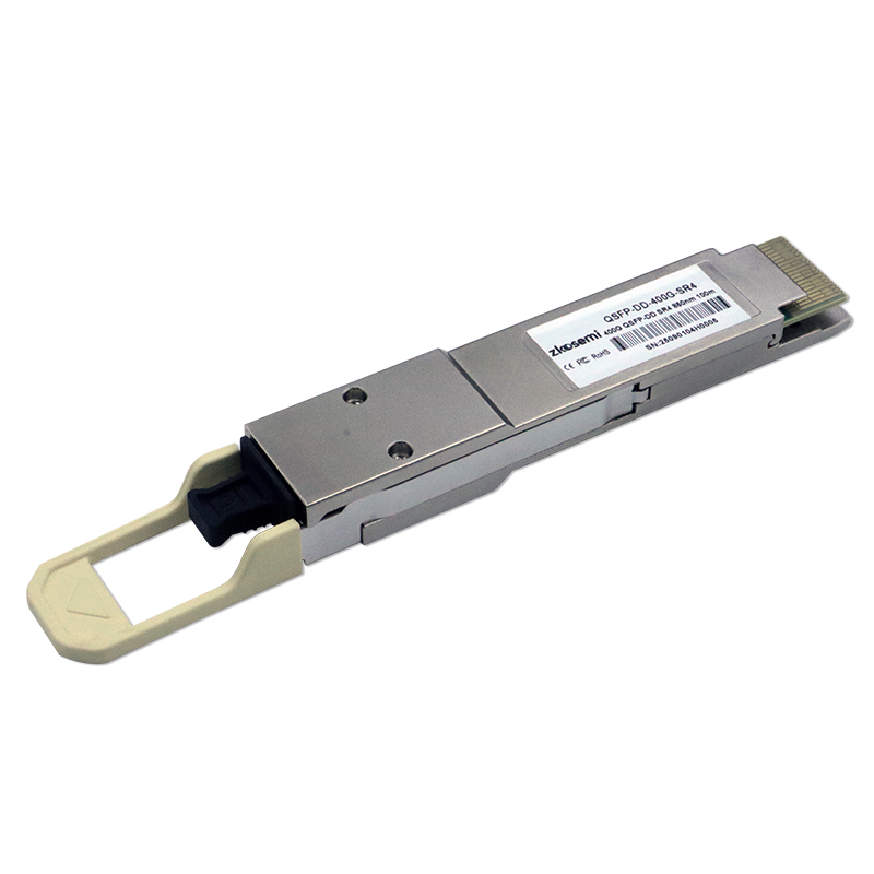
400GBASE SR4 QSFP-DD 850nm 50m MPO-12/APC DDM MMF Optical Transceiver Module
ZK-QDD-400G-SR4
400Gbps QSFP-DD SR4 850nm 100m MMF Transceiver
Features
n Support 100GBASE per lane in multi mode fiber
n Data rate up to 425Gb ps (4 x 106.25 Gb ps)
n Reach up to 100m on MMF (OM4)
n 850nm VCSEL laser and PIN receiver
n High speed I/O electrical interface (400GAUI-8) .
n Single MPO-12 receptacle
n Operating case temperature: 0 to +70°C
n Compliant to RoHS 6/6
n Compliant to QSFP-DD MSA and CMIS5.0
Applications
n Data Center Interconnect
n 400G Ethernet
n Infiniband interconnects
n Enterprise networking
Description
This module is a hot pluggable fiber optic transceiver in the QSFP-DD form factor with digital diagnostics monitoring functionality (DDM) and control function. The 400G QSFP-DD SR4 module has four identical and independent lanes which provides a point-to-point 400Gb/s link over OM4 multi mode fiber up to 100m. This makes it an ideal low-cost solution for short reach data center optical interconnects.
The central wavelength of each lane is at 850nm wavelength. The low power consumption and excellent EMI performance enable system design with high port density.
The transceiver can be conveniently assembled into and released from the host system through the latch.
The transceiver operates from a single +3.3V power supply over an operating case temperature range of 0℃ to +70℃. The housing is made of metal for EMI immunity.
Absolute Maximum Ratings
Parameter | Symbol | Min | Max | Units | Notes |
Case Operating Temperature | TOP | 0 | 70 | °C | 1,2 |
Power Supply Voltage | Vcc | -0.5 | 3.6 | V | |
Storage Temperature Range | TST | -40 | 85 | °C | 1,2 |
Operating Relative Humidity | RH | 5 | 85 | % | 1,2,3 |
Notes:
1. Absolute Maximum Ratings are those beyond which damage to the device may occur.
2. Between the Recommended Operating conditions and Absolute Maximum ratings, prolonged operation is not intended, and permanent device degradation may occur.
3. Non-condensing.
Optical Characteristics
Parameter | Symbol | Min | Typical | Max | Units |
Transmitter | |||||
Signaling rate, each lane | 53.125 ± 100 ppm | GBd | |||
Modulation format | PAM4 | ||||
Center wavelength | λC | 842 | - | 948 | nm |
RMS spectral width1 | - | - | - | 0.65 | nm |
Average launch power, each lane | AOPL | –4.6 | - | 4 | dBm |
Outer Optical Modulation Amplitude (OMAouter), each lane | TOMA | - | - | 3.5 | dBm |
Outer Optical Modulation Amplitude(OMAouter), each lane for max(TECQ, TDECQ) ≤1.8 dB for 1.8<max(TECQ, TDECQ) ≤4.4 dB |
TOMA |
-
–2.6 –4.4 |
- |
- |
dBm |
Transmitter and dispersion eye closure for PAM4 (TDECQ), each lane | TDECQ | - | - | 4.4 | dB |
Transmitter eye closure for PAM4 (TECQ), each lane | TECQ | - | - | 4.4 | dB |
Overshoot/undershoot | - | - | - | 26 | % |
Transmitter power excursion, each lane | - | - | - | 2 | dBm |
Extinction Ratio | ER | 2.5 | - | - | dB |
Transmitter transition time, each lane | - | - | - | 17 | ps |
Average launch power of OFF transmitter, each lane | TOFF | - | - | -30 | dBm |
RIN12OMA | RIN | - | - | -131 | dB/Hz |
Optical return loss tolerance | ORL | - | - | 14 | dB |
Encircled flux2 | ≥86% at 9nm ≤30% at 45µm | ||||
Receiver | |||||
Signaling rate, each lane | 53.125 ± 100 ppm | GBd | |||
Modulation format | PAM4 | ||||
Center wavelength | λC | 842 | - | 948 | nm |
Damage threshold1 | AOPD | 5 | - | dBm | |
Average receive power, each lane2 | AOPR | -6.3 | - | 4 | dBm |
Receive power, each lane (OMAouter) | OMAR | - | - | 3.5 | dBm |
Receiver reflectance | RR | - | - | -15 | dB |
Receiver sensitivity (OMAouter), each lane for TECQ≤1.8 dB for 1.8<TECQ≤4.4 dB | SOMA |
- |
- | - -4.4 -6.2 | dBm |
Stressed receiver sensitivity (OMAouter), each lane | SRS | - | - | -1.8 | dBm |
Conditions of stressed receiver sensitivity test:3 | |||||
Stressed eye closure for PAM4 (SECQ) | - | - | 4.4 | - | dB |
OMAouter of each aggressor lane | - | - | 3.5 | - | dBm |
Notes:
1. RMS spectral width is the standard deviation of the spectrum
2. If measured into type A 1a.2 or type A 1a.3, or A 1a.4, 50 μm fiber, in accordance with IEC 61280-1-4
3. The receiver shall be able to tolerate, without damage, continuous exposure to an optical input signal having this average power level on one lane. The receiver does not have to operate correctly at this input power.
4. Average receive power, each lane (min) is informative and not the principal indicator of signal strength. A received power below this value cannot be compliant; however, a value above this does not ensure compliance.
5. These test conditions are for measuring stressed receiver sensitivity. They are not characteristics of the receiver.
Electrical Characteristics
Parameter | Symbol | Min | Typical | Max | Units |
Power Supply Voltage | VCC1, VCCTx, | 3.13 | 3.30 | 3.47 | V |
Power Consumption | PW | - | - | 7 | W |
Power Consumption-LP mode | - | - | - | 1.5 | W |
Transmitter | |||||
Signaling rate, each lane | 26.5625 ± 100 ppm | GBd | |||
Differential pk-pk input voltage tolerance | - | 900 | - | - | mV |
Differential termination mismatch | - | - | - | 10 | % |
Single-ended voltage tolerance range | - | –0.4 | - | 3.3 | V |
DC common-mode voltage | - | –350 | - | 2850 | mV |
Receiver | |||||
Signaling rate, each lane | 26.5625 ± 100 ppm | GBd | |||
AC common-mode output voltage RMS | - | - | - | 17.5 | mV |
Differential peak-to-peak output voltage | - | - | - | 900 | mV |
Near-end eye symmetry mask width | ESMW | - | 0.265 | - | uI |
Near-end eye height, differential | EH | 70 | - | - | mV |
Far-end eye symmetry mask width | ESMW | - | 0.2 | - | uI |
Far-end eye height, differential | EH | 30 | - | - | mV |
Far-end pre-cursor ISI ratio | - | -4.5 | - | 2.5 | % |
Differential termination mismatch | - | - | - | 10 | % |
Transition time, 20-80% | - | 9.5 | - | - | ps |
DC common mode voltage | - | -350 | - | 2850 | mV |
Pin Description

Pin | Logic | Symbol | Description | Plug Sequence |
1 | GND | Ground | 1B | |
2 | CML - I | Tx2n | Transmitter Inverted Data Input | 3B |
3 | CML - I | Tx2p | Transmitter Non-Inverted Data Input | 3B |
4 | GND | Ground | 1B | |
5 | CML - I | Tx4n | Transmitter Inverted Data Input | 3B |
6 | CML - I | Tx4p | Transmitter Non-Inverted Data Input | 3B |
7 | GND | Ground | 1B | |
8 | LVTTL - I | ModSelL | Module Select | 3B |
9 | LVTTL - I | ResetL | Module Reset | 3B |
10 | VccRx | +3.3V Power Supply Receiver | 2B | |
11 | LVCMOS - I /O | SCL | TWI serial interface clock | 3B |
12 | LVCMOS - I/O | SDA | TWI serial interface data | 3B |
13 | GND | Ground | 1B | |
14 | CML - O | Rx3p | Receiver Non-Inverted Data Output | 3B |
15 | CML - O | Rx3n | Receiver Inverted Data Output | 3B |
16 | GND | Ground | 1B | |
17 | CML - O | Rx1p | Receiver Non-Inverted Data Output | 3B |
18 | CML - O | Rx1n | Receiver Inverted Data Output | 3B |
19 | GND | Ground | 1B | |
20 | GND | Ground | 1B | |
21 | CML - O | Rx2n | Receiver Inverted Data Output | 3B |
22 | CML - O | Rx2p | Receiver Non-Inverted Data Output | 3B |
23 | GND | Ground | 1B | |
24 | CML - O | Rx4n | Receiver Inverted Data Output | 3B |
25 | CML - O | Rx4p | Receiver Non-Inverted Data Output | 3B |
26 | GND | Ground | 1B | |
27 | LVTTL - O | Mod PrsL | Module Present | 3B |
28 | LVTTL - O | IntL / RxLOS | Interrupt /optional RxLOS | 3B |
29 | VccTx | +3.3V Power supply transmitter | 2B | |
30 | Vcc1 | +3.3V Power supply | 2B | |
31 | LVTTL - I | LPMode /TxDis | Low Power mode/optional TX Disable | 3B |
32 | GND | Ground | 1B | |
33 | CML - I | Tx3p | Transmitter Non-Inverted Data Input | 3B |
34 | CML - I | Tx3n | Transmitter Inverted Data Input | 3B |
35 | GND | Ground | 1B | |
36 | CML - I | Tx1p | Transmitter Non-Inverted Data Input | 3B |
37 | CML - I | Tx1n | Transmitter Inverted Data Input | 3B |
38 | GND | Ground | 1B | |
39 | GND | Ground | 1A | |
40 | CML - I | Tx6n | Transmitter Inverted Data Input | 3A |
41 | CML - I | Tx6p | Transmitter Non-Inverted Data Input | 3A |
42 | GND | Ground | 1A | |
43 | CML - I | Tx8n | Transmitter Inverted Data Input | 3A |
44 | CML - I | Tx8p | Transmitter Non-Inverted Data Input | 3A |
45 | GND | Ground | 1A | |
46 | LVCMOS/CML - I | P/VS4 | Programmable/Module Vendor Specific 4 | 3A |
47 | LVCMOS/CML - I | P/ VS1 | Programmable/Module Vendor Specific 1 | 3A |
48 | VccRx1 | 3.3V Power Supply | 2A | |
49 | LVCMOS/CML - O | P/ VS2 | Programmable/Module Vendor Specific 2 | 3A |
50 | LVCMOS/CML - O | P/ VS3 | Programmable/Module Vendor Specific 3 | 3A |
51 | GND | Ground | 1A | |
52 | CML - O | Rx7p | Receiver Non-Inverted Data Output | 3A |
53 | CML - O | Rx7n | Receiver Inverted Data Output | 3A |
54 | GND | Ground | 1A | |
55 | CML - O | Rx5p | Receiver Non-Inverted Data Output | 3A |
56 | CML - O | Rx5n | Receiver Inverted Data Output | 3A |
57 | GND | Ground | 1A | |
58 | GND | Ground | 1A | |
59 | CML - O | Rx6n | Receiver Inverted Data Output | 3A |
60 | CML - O | Rx6p | Receiver Non-Inverted Data Output | 3A |
61 | GND | Ground | 1A | |
62 | CML - O | Rx8n | Receiver Inverted Data Output | 3A |
63 | CML - O | Rx8p | Receiver Non-Inverted Data Output | 3A |
64 | GND | Ground | 1A | |
65 | NC | No Connect | 3A | |
66 | Reserved | For future use | 3A | |
67 | VccTx1 | 3.3V Power Supply | 2A | |
68 | Vcc2 | 3.3V Power Supply | 2A | |
69 | L VCMOS - I | ePPS/Clock | 1PPS PTP clock or reference clock input | 3A |
70 | GND | Ground | 1A | |
71 | CML-I | Tx7p | Transmitter Non-Inverted Data Input | 3A |
72 | CML-I | Tx7n | Transmitter Inverted Data Input | 3A |
73 | GND | Ground | 1A | |
74 | CML-I | Tx5p | Transmitter Non-Inverted Data Input | 3A |
75 | CML-I | Tx5n | Transmitter Inverted Data Input | 3A |
76 | GND | Ground | 1A |
Mechanical Dimensions

Important Notice
Performance figures, data and any illustrative material provided in this data sheet are typical and must be specifically confirmed in writing by Zkosemi before they become applicable to any particular order or contract. In accordance with the Zkosemi policy of continuous improvement specifications may change without notice. The publication of information in this data sheet does not imply freedom from patent or other protective rights of Zkosemi or others. Further details are available from any Zkosemi sales representative.