

Product type
 Contact Information
+86 755 89660635
+86 189 2461 3736

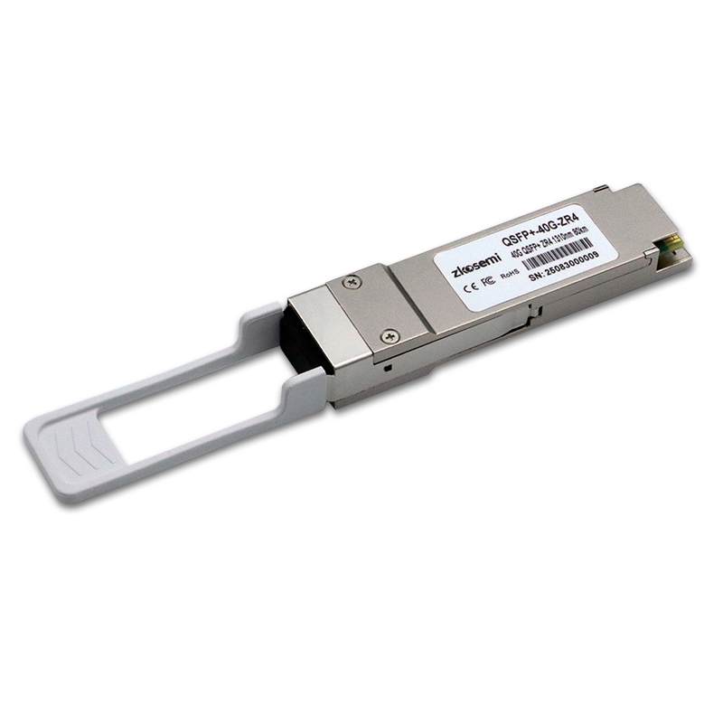
40Gbps QSFP+ ZR4 1310nm 80km SMF Transceiver
ZK-QSFP+-40G-ER4
40Gbps QSFP+ ZR4 1310nm 80km SMF Transceiver
Features
n Support line rates for 41.25 Gb/s;
n Lane bit rate 10.3125 Gb/s 40GE
n Up to 80km transmission on single mode fiber
n LAN WDM EML laser and APD
n Support Multi-Pin function with IntL/RxLOSL and LPMode/TxDIS
n High speed I/O electrical interface (CAUI-4)
n I2C interface with integrated Digital Diagnostic monitoring
n QSFP+ MSA package with duplex LC connector
n Single +3.3V power supply
n Power dissipation
n Commercial:< 4.5W
n Industrial:< 5.5W
n Complies with EU Directive 2015/863/EU
Applications
n Data centers Switches and Routers
n Metro networks
n Switches and Routers
n 40G BASE-ZR4
Descriptions
ZK-QSFP+-40G-ER4 is designed for 80km optical communication applications. Optical transceiver integrates the transmit and receive path onto one module. On the transmit side, four lanes of serial data streams are recovered, retimed and passed on to four laser drivers, which control four electric-absorption modulated lasers (Lan-WDM) with 1296, 1300, 1305, and 1309 nm center wavelengths. The optical signals are then multiplexed into a single-mode fiber through an industry-standard LC connector. On the receive side, four lanes of optical data streams are optically De multiplexed by an integrated optical De multiplexer. And passed on to an output driver, the receiver adopts APD. This module features a hot-pluggable electrical interface, low power consumption, and 2-wire serial interface.
Absolute Maximum Ratings
It has to be noted that the operation in excess of any individual absolute maximum ratings might cause permanent damage to this module.
Parameter | Symbol | Min | Max | Unit | Notes |
Storage Temperature | TS | -40 | 85 | deg°C | |
Operating Case Temperature | TOP | -40 | 85 | deg°C | |
Power Supply Voltage | VCC | -0.5 | 3.6 | V | |
Damage Threshold, each Lane | THd | -2.5 | dBm | ||
Relative Humidity (non-condensation) | RH | 0 to 85% non-condensing | % | ||
Recommended Operating Conditions
Parameter | Symbol | Min | Typ | Max | Unit | Notes |
Operating Case Temperature | Top | 0 | +70 | °C | Commercial | |
-40 | +85 | Industrial | ||||
Power Supply Voltage | VCC | 3.14 | 3.3 | 3.47 | V | |
Maximum Power Dissipation | PD | 4.5 | W | Commercial | ||
Maximum Power Dissipation | PD | 5.5 | W | Industrial | ||
Lane Bit Rate | 10.3125 | Gb/s | ||||
Transmission Distance | TD | 40 | km | |||
Coupled fiber | Single mode fiber | 1 | ||||
Notes:
1. Optical fiber use 9/125um SMF。
Electrical Characteristics
The following electrical characteristics are defined over the Recommended Operating Environment unless otherwise specified.
Parameter | Test Point | Min | Typ | Max | Unit | Notes |
Transmitter (Module Input) | ||||||
Data Rate, each lane | 10.3125 | Gbps | ||||
Differential Voltage pk-pk | Vpp | 900 | Mv | 1 | ||
Common Mode Voltage | Vcm | -350 | 2850 | Mv | ||
Transition time | Trise/Tfall | 10 | ps | 2 | ||
Receiver (Module Output) | ||||||
Data Rate, each lane | 10.3125 | |||||
Common Mode Noise, RMS | Vrms | 17.5 | Mv | |||
Differential output voltage swing | Vout, pp | 900 | Mv | |||
Eye width | EW15 | 0.57 | UI | |||
Eye height | EH15 | 228 | mV | |||
Differential Termination Resistance Mismatch | 10 | % | 1 | |||
Transition time | Trise/Tfall | 12 | ps | |||
Common Mode Noise, RMS | Vrms | 17.5 | Mv | |||
Notes:
1. At 1 MHz.
2. 20%~80%.
Optical and Characteristics
Parameter | Symbol | Min | Typ | Max | Unit | Note |
Transmitter | ||||||
Signaling Speed per Lane | 10.3125 | Gbps | ||||
Center Wavelength Lane 0 | λ0 | 1294.53 | 1295.56 | 1296.59 | nm | |
Center Wavelength Lane 1 | λ1 | 1299.02 | 1300.05 | 1301.09 | nm | |
Center Wavelength Lane 2 | λ2 | 1303.54 | 1304.58 | 1305.63 | nm | |
Center Wavelength Lane 3 | λ3 | 1308.09 | 1309.14 | 1310.19 | nm | |
Total Launch Power,40GE | PT | 12.5 | dBm | 1 | ||
Average Launch Power per Lane, | Pavg | 1 | 6.5 | dBm | 1 | |
OMA, each Lane | POMA | 2 | 6.5 | dBm | 1 | |
Difference in launch power between any two lanes(Average and OMA) between any Two Lanes (OMA) | Ptx,diff | 3 | Db | |||
Average Output Power (Laser Turn off) | Poff | -30 | dBm | |||
Side Mode Suppression Ratio | SMSR | 30 | Db | |||
Extinction Ratio, 100GE | ER | 8.2 | Db | |||
RIN20OMA | RIN | -130 | Db/Hz | |||
Optical Return Loss Tolerance | TOL | 20 | Db | |||
Transmitter Reflectance | RT | -12 | Db | |||
Optical Eye Mask | {0.25,0.4, 0.45, 0.25, 0.28, 0.4} | % | ||||
Receiver | ||||||
Signaling rate, each lane | 10.3125 | Gbps | ||||
Center Wavelength Lane 0 | λ0 | 1294.53 | 1295.56 | 1296.59 | nm | |
Center Wavelength Lane 1 | λ1 | 1299.02 | 1300.05 | 1301.09 | nm | |
Center Wavelength Lane 2 | λ2 | 1303.54 | 1304.58 | 1305.63 | nm | |
Center Wavelength Lane 3 | λ3 | 1308.09 | 1309.14 | 1310.19 | nm | |
Damage threshold , each lane | Pd amage | -2.5 | dBm | |||
Average power at receiver input , each lane | R | -24 | -6 | dBm | 2 | |
Los Assert | LosA | -35 | dBm | |||
Los De-assert | LosDA | -25 | dBm | |||
Los Hysteresis | LosH | 0.5 | dB | |||
Notes:
1. The optical power is launched into SMF。
2. Measured with a PRBS 231-1 test pattern @10.3125 Gb/s, PRBS 2^31-1.
Digital Diagnostics
Parameter | Unit | Specification |
Temperature Monitor absolute error | ℃ | ± 3.0 |
Supply Voltage Monitor absolute error | % | ± 5 |
I_bias Monitor absolute error | % | ± 10 |
Received Power (Rx) Monitor absolute error | dB | ± 3.0 |
Transmit Power (Tx) Monitor absolute error | dB | ± 3.0 |
Module Block Diagram
Pin Diagram
Pin Definitions
PIN | Logic | Symbol | Description | Plug Seq. | Notes |
1 | GND | Ground | 1 | 1 | |
2 | CML-I | Tx2n | Transmitter Inverted Data Input | 3 | |
3 | CML-I | Tx2p | Transmitter Non-Inverted Data output | 3 | |
4 | GND | Ground | 1 | 1 | |
5 | CML-I | Tx4n | Transmitter Inverted Data Input | 3 | |
6 | CML-I | Tx4p | Transmitter Non-Inverted Data output | 3 | |
7 | GND | Ground | 1 | 1 | |
8 | LVTLL-I | ModSelL | Module Select | 3 | |
9 | LVTLL-I | ResetL | Module Reset | 3 | |
10 | VccRx | ﹢3.3V Power Supply Receiver | 2 | 2 | |
11 | LVCMOS-I/O | SCL | 2-Wire Serial Interface Clock | 3 | |
12 | LVCMOS-I/O | SDA | 2-Wire Serial Interface Data | 3 | |
13 | GND | Ground | 1 | ||
14 | CML-O | Rx3p | Receiver Non-Inverted Data Output | 3 | |
15 | CML-O | Rx3n | Receiver Inverted Data Output | 3 | |
16 | GND | Ground | 1 | 1 | |
17 | CML-O | Rx1p | Receiver Non-Inverted Data Output | 3 | |
18 | CML-O | Rx1n | Receiver Inverted Data Output | 3 | |
19 | GND | Ground | 1 | 1 | |
20 | GND | Ground | 1 | 1 | |
21 | CML-O | Rx2n | Receiver Inverted Data Output | 3 | |
22 | CML-O | Rx2p | Receiver Non-Inverted Data Output | 3 | |
23 | GND | Ground | 1 | 1 | |
24 | CML-O | Rx4n | Receiver Inverted Data Output | 3 | 1 |
25 | CML-O | Rx4p | Receiver Non-Inverted Data Output | 3 | |
26 | GND | Ground | 1 | 1 | |
27 | LVTTL-O | ModPrsL | Module Present | 3 | |
28 | LVTTL-O | IntL/Rx_LOS | Interrupt/Rx_LOS | 3 | |
29 | VccTx | +3.3 V Power Supply transmitter | 2 | 2 | |
30 | Vcc1 | +3.3 V Power Supply | 2 | 2 | |
31 | LVTTL-I | LPMode/TxDIS | Low Power Mode/Tx_Disable | 3 | |
32 | GND | Ground | 1 | 1 | |
33 | CML-I | Tx3p | Transmitter Non-Inverted Data Input | 3 | |
34 | CML-I | Tx3n | Transmitter Inverted Data Output | 3 | |
35 | GND | Ground | 1 | 1 | |
36 | CML-I | Tx1p | Transmitter Non-Inverted Data Input | 3 | |
37 | CML-I | Tx1n | Transmitter Inverted Data Output | 3 | |
38 | GND | Ground | 1 | 1 |
Notes:
1. GND is the symbol for signal and supply (power) common for the QSFP28 module. All are common within the QSFP28 module and all module voltages are referenced to this potential unless otherwise noted. Connect these directly to the host board signal-common ground plane.
2. Vcc Rx, Vcc1 and Vcc Tx are the receiver and transmitter power supplies and shall be applied concurrently. Requirements defined for the host side of the Host Edge Card Connector are listed in MSA. The connector pins are each rated for a maximum current of 1000 Ma
Recommended Interface Circuit
Mechanical Dimensions
Important Notice
Performance figures, data and any illustrative material provided in this data sheet are typical and must be specifically confirmed in writing by Zkosemi before they become applicable to any particular order or contract. In accordance with the Zkosemi policy of continuous improvement specifications may change without notice. The publication of information in this data sheet does not imply freedom from patent or other protective rights of Zkosemi or others. Further details are available from any Zkosemi sales representative