

Product type
 Contact Information
+86 755 89660635
+86 189 2461 3736

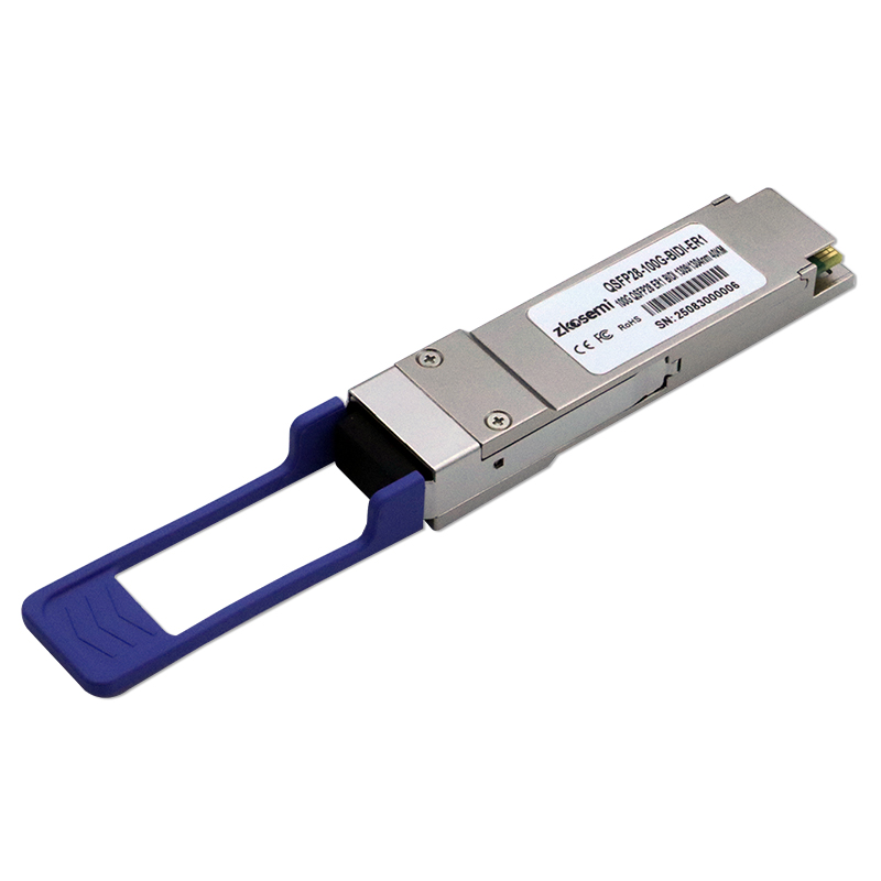
100Gbps QSFP28 BIDI ER1 40km SMF Transceiver
ZK-QSFP28-100G-BX40
100Gbps QSFP28 BIDI ER1 40km SMF Transceiver
Features
n Supports 100GBASE-ER1 BIDI
n Lane signaling rate 106.25Gb/s with PAM4
n Up to 40km transmission on SMF
n EML Laser and APD receiver
n 4x25.78Gb/s with NRZ electrical interface (CAUI-4)
n Support KP4 FEC inside the module
n High speed I/O electrical interface
n I2C interface with integrated Digital Diagnostic monitoring
n QSFP28 MSA package with simplex LC connector
n Single +3.3V power supply
n Power consumption <4W
n Operating case temperature: 0 to +70 °C
n Compliant to 802.3cu, SFF-8636&SFF-8679 standard
n Compliant to 100G Lambda MSA 100G-ER1 Optical Specifications
n Complies with EU Directive 2015/863/EU
Applications
n Data Center
n 100 Gigabit Ethernet
Descriptions
The 100G QSFP28 ER1 BIDI is designed for 40km optical communication applications. It is intended for the service with single mode fiber in 100Gb/s high speed data communications. The optical signals are multiplexed to a single-mode fiber through commercial standard LC connector.
Ordering Information
Part No. | Date Rate | Wavelength | Distance | Temp | DDMI |
ZK-QSFP28-100G-BX40-U | 106.25Gb ps | Tx1305/Rx1309 | 40km | 0~70℃ | Yes |
ZK-QSFP28-100G-BX40-D | 106.25Gb ps | Tx1309/Rx1305 | 40km | 0~70℃ | Yes |
Module Block Diagram
Absolute Maximum Ratings
Parameter | Symbol | Min. | Typical | Max. | Unit | Notes |
Storage Temperature | TS | -40 | - | +85 | °C | |
Supply Voltage | VCC | -0.5 | - | +4.0 | V | |
Operating Relative Humidity | RH | - | - | +85 | % |
Recommended Operating Conditions
Parameter | Symbol | Min. | Typical | Max. | Unit | Notes |
Operating Case Temperature | TC | 0 | - | +70 | °C | |
Power Supply Voltage | VCC | 3.13 | 3.3 | 3.47 | V | |
Power consumption | ICC | 4 | W | |||
Transmission Distance | TD | - | - | 40 | km | Over SMF |
Electrical Characteristics
Parameter | Symbol | Min. | Typical | Max. | Unit |
Input Differential Impedance | Rin | - | 100 | - | Ohm |
Differential Data Input Amplitude | VIN,P-P | - | 900 | mVpp | |
Differential termination mismatch (max) | D-mismatch | - | - | 10 | % |
DC common-mode input voltage | -0.3 | - | 2.8 | V | |
Transition time(20%~80%) | Tr Tf | 10 | - | - | ps |
LPMode, Reset and ModSelL / Tx dis | VIL | -0.3 | - | 0.8 | V |
LPMode, Reset and ModSelL / Tx dis | VIH | 2.0 | - | VCC+0.3 | V |
Output Differential Impedance | Rout | - | 100 | - | Ohm |
Differential Data Output Amplitude | VOUTP-P | - | - | 900 | mVpp |
Differential termination mismatch (max) | D-mismatch | - | - | 10 | % |
Transition time, 20% to 80% | Tr Tf | 12 | - | ps | |
Mod PrsL and IntL/ Rx los | VOL | 0 | - | 0.4 | V |
Mod PrsL and IntL/ Rx los | VOH | VCC-0.5 | - | VCC+0.3 | V |
Optical and Characteristics
Parameter | Symbol | Min. | Typical | Max. | Unit | Notes |
Transmitter | ||||||
Center Wavelength | CW | 1303.54 | 1304.58 | 1305.63 | nm | |
1308.09 | 1309.14 | 1310.19 | nm | |||
Signaling Rate | SR | 53.125 | GBd | |||
Frequency Offset | Foffset | -100 | 100 | ppm | ||
Average Launch Power | PTX | 1.7 | - | 7.1 | dBm | 1 |
Transmitter and dispersion eye closure for PAM4 (TDECQ) (max) | TDECQ |
- |
- | 3.9 | dBm | |
Average Output Power (Laser Turn off) | Poff |
- |
- | -30 | dBm | |
Side Mode Suppression Ratio | SMSR | 30 | - | - | dB | |
Extinction Ratio | ER | 5 | - | - | dB | |
RIN_OMA | RIN | - | - | -136 | dB/Hz | |
Transmitter reflectance | Tref | - | - | -26 | dB | |
Optical Return Loss Tolerance | ORLT | - | - | 15.6 | dB | |
Receiver | ||||||
Center Wavelength | CW | 1303.54 | 1304.58 | 1305.63 | nm | |
1308.09 | 1309.14 | 1310.19 | nm | |||
Damage threshold | Pdamage | -2.4 | - | - | dBm | 2 |
Average Rx Power | PRx | -16 | - | -3.4 | dBm | 3 |
Receive power _OMAouter | POMA | - | - | -2.6 | dBm | |
Receiver sensitivity _OMAouter for TDECQ < 1.4 dB for 1.4 dB ≤ TDECQ ≤ 3.4 dB |
SEN _OMA |
- |
- | -13.8 -15.2+TECQ |
dBm |
4 |
Reflectance | Ref | - | - | -26 | dB | |
Los Assert | LosA | -30 | - | dBm | ||
Los De-Assert | LosDA | - | - | -13 | dBm | |
Los Hysteresis | LosH | 0.5 | - | - | dB | |
Notes:
1. The optical power is launched into SMF.
2. The receiver shall be able to tolerate, without damage, continuous exposure to an optical input signal having this average power level. The receiver does not have to operate correctly at this input power.
3. Average receive power, each lane (min) is informative and not the principal indicator of signal strength.
4. Measured with conformance test signal at TP3 using the test pattern PRBS31Q or scrambled idle for stressed receiver sensitivity for the BER= 2.4x10⁻⁴.
Digital Diagnostics
Parameter | Range | Accuracy | Unit | Calibration |
Temperature | 0 to 70 | ±3 | ºC | Internal |
Voltage | 0 to Vcc | ±3% | V | Internal |
Tx Bias Current | 0 to 100 | ±10% | mA | Internal |
Tx Output Power | 1.7 to 7.1 | ±3 | dB | Internal |
Rx Input Power | -16 to -3.4 | ±3 | dB | Internal |
Recommended Interface Circuit
Pin Diagram
Pin Definitions
PIN | Logic | Symbol | Description | Notes |
1 | GND | Ground | 1 | |
2 | CML-I | Tx2n | Transmitter Inverted Data Input | |
3 | CML-I | Tx2p | Transmitter Non-Inverted Data output | |
4 | GND | Ground | 1 | |
5 | CML-I | Tx4n | Transmitter Inverted Data Input | |
6 | CML-I | Tx4p | Transmitter Non-Inverted Data output | |
7 | GND | Ground | 1 | |
8 | LVTLL-I | ModSelL | Module Select | |
9 | LVTLL-I | ResetL | Module Reset | |
10 | VccRx | +3.3V Power Supply Receiver | 2 | |
11 | LVCMOS-I/O | SCL | 2-Wire Serial Interface Clock | |
12 | LVCMOS-I/O | SDA | 2-Wire Serial Interface Data | |
13 | GND | Ground | ||
14 | CML-O | Rx3p | Receiver Non-Inverted Data Output | |
15 | CML-O | Rx3n | Receiver Inverted Data Output | |
16 | GND | Ground | 1 | |
17 | CML-O | Rx1p | Receiver Non-Inverted Data Output | |
18 | CML-O | Rx1n | Receiver Inverted Data Output | |
19 | GND | Ground | 1 | |
20 | GND | Ground | 1 | |
21 | CML-O | Rx2n | Receiver Inverted Data Output | |
22 | CML-O | Rx2p | Receiver Non-Inverted Data Output | |
23 | GND | Ground | 1 | |
24 | CML-O | Rx4n | Receiver Inverted Data Output | 1 |
25 | CML-O | Rx4p | Receiver Non-Inverted Data Output | |
26 | GND | Ground | 1 | |
27 | LVTTL-O | Mod PrsL | Module Present | |
28 | LVTTL-O | IntL/Rx_LOS | Interrupt/Rx_LOS | 3 |
29 | VccTx | +3.3 V Power Supply transmitter | 2 | |
30 | Vcc1 | +3.3 V Power Supply | 2 | |
31 | LVTTL-I | LPMode/TxDIS | Low Power Mode/Tx_Disable | 3 |
32 | GND | Ground | 1 | |
33 | CML-I | Tx3p | Transmitter Non-Inverted Data Input | |
34 | CML-I | Tx3n | Transmitter Inverted Data Output | |
35 | GND | Ground | 1 | |
36 | CML-I | Tx1p | Transmitter Non-Inverted Data Input | |
37 | CML-I | Tx1n | Transmitter Inverted Data Output | |
38 | GND | Ground | 1 |
Notes:
1. GND is the symbol for signal and supply (power) common for the QSFP28 module. All are common within the QSFP28 module and all module voltages are referenced to this potential unless otherwise noted. Connect these directly to the host board signal-common ground plane.
2. Vcc Rx, Vcc1 and Vcc Tx are the receiver and transmitter power supplies and shall be applied concurrently. Requirements defined for the host side of the Host Edge Card Connector are listed in MSA. The connector pins are each rated for a maximum current of 1000 mA.
3. Two Multi-Purpose Pin for supporting Tx_DIS and Rx_LOS function in the 100G QSFP28 ER1 BIDI module
Mechanical Dimensions
Important Notice
Performance figures, data and any illustrative material provided in this data sheet are typical and must be specifically confirmed in writing by Zkosemi before they become applicable to any particular order or contract. In accordance with the Zkosemi policy of continuous improvement specifications may change without notice. The publication of information in this data sheet does not imply freedom from patent or other protective rights of Zkosemi or others. Further details are available from any Zkosemi sales representative