

Product type
 Contact Information
+86 755 89660635
+86 189 2461 3736

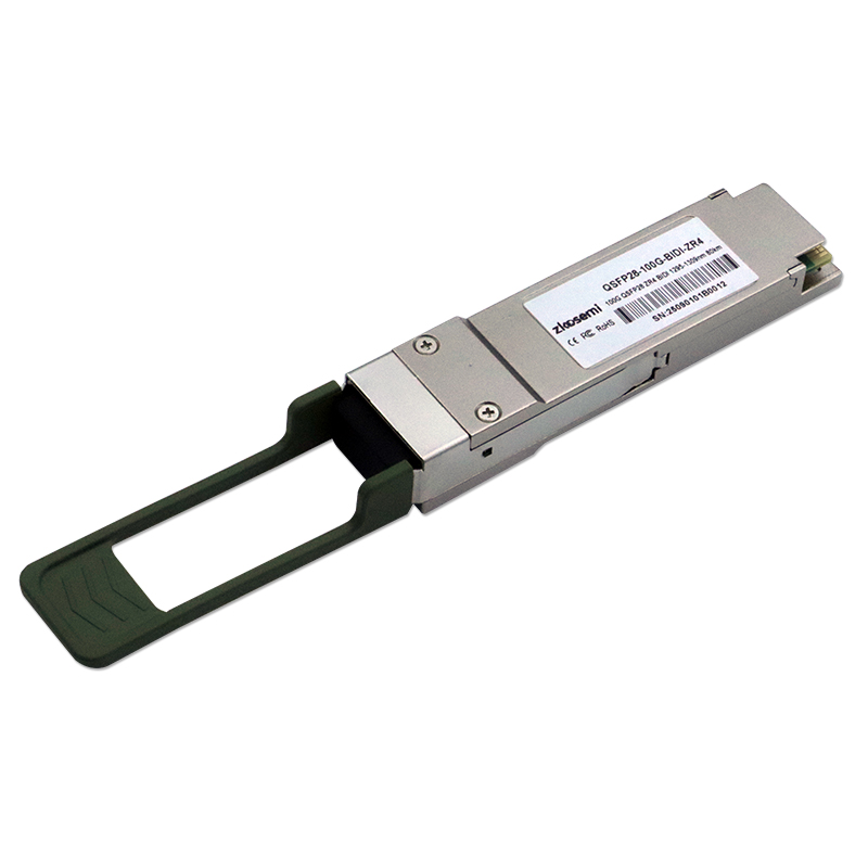
100Gbps QSFP28 BIDI ZR4 80km SMF Transceiver
ZK-QSFP28-100G-BX80
100Gbps QSFP28 BIDI ZR4 80km SMF Transceiver
Features
n Supports 103.125Gb/s aggregate bit rate
n Built-in 4-channel Clock and Data Recovery (CDR) in TX and RX
n LAN WDM EML laser and PIN receiver with SOA
n Up to 80km reach for G.652 SMF
n Hot pluggable 38 pin electrical interface
n QSFP28 MSA compliant
n BIDI LC optical receptacle
n RoHS-10 compliant and lead-free
n Excellent EMI performance
n Single +3.3V power supply
n Maximum power consumption 5.5W
n Case operating temperature:0 ~ 70℃
Applications
n 100GBASE-ZR4 Ethernet Links
n Infiniband QDR and DDR interconnects
n Telecom networking
Descriptions
100G-QSFP28-BIDI-ZR4 is designed for 80km optical communication applications. This module contains 4-lane optical transmitter, 4-lane optical receiver and module management block including 2 wire serial inter-face. The optical signals are multiplexed to a single-mode fiber through an industry standard LC connector.
Ordering information
Part No. | Date Rate | Wavelength | Distance | Temp | DDMI |
ZK-QSFP28-100G-BX80-U | 106.25Gb ps | Tx1273~1286nm/ Rx1295~1309nm | 80km | 0~70℃ | Yes |
ZK-QSFP28-100G-BX80-D | 106.25Gb ps | Tx1295~1309nm/ | 80km | 0~70℃ | Yes |
Absolute Maximum Ratings
Parameter | Symbol | Min | Max | Unit | Notes |
Storage Temperature | TS | -40 | 85 | ℃ | |
Power Supply Voltage | VCC | -0.3 | 4.0 | V | |
Relative Humidity (non-condensation) | RH | 15 | 85 | % | |
Damage Threshold | THd | 6.5 | dBm |
Recommended Operating Conditions
Parameter | Symbol | Min | Typical | Max | Unit | Notes |
Operating Case Temperature | TOP | 0 | 70 | ℃ | ||
Power Supply Voltage | VCC | 3.135 | 3.3 | 3.465 | V | |
Data Rate, each Lane | 25.78125 | Gb/s | ||||
Control Input Voltage High | 2 | Vcc | V | |||
Control Input Voltage Low | 0 | 0.8 | V | |||
Link Distance (SMF) | D | 80 | km |
Electrical Characteristics
Parameter | Symbol | Min. | Typ. | Max | Unit | Notes |
Power Consumption | p | 5.5 | W | |||
Supply Current | Icc | 1585 | mA | |||
Transmitter (each Lane) | ||||||
Input differential impedance | Rin | 100 | Ω | |||
Differential Termination Mismatch |
10 |
% | ||||
Differential Data Input Amplitude |
Vin, PP |
180 |
1000 |
mV | ||
LPMode, Reset and ModSelL | VIL | -0.3 | 0.8 | V | ||
VIH | 2 | Vcc+0.3 | V | |||
Receiver | ||||||
Differential Data Output Amplitude |
Vout, PP |
350 |
900 |
mV | ||
Differential Termination Mismatch |
10 |
% | ||||
Transition Time, 20 to 80% | 9.5 | ps | ||||
Mod PrsL and IntL | VOL | 0 | 0.4 | V | ||
VOH | Vcc-0.5 | Vcc+0.3 | V | |||
Optical Characteristics
Parameter | Symbol | Min. | Typical | Max | Unit | Notes |
Transmitter | ||||||
Center wavelength | L0 | 1272.55 | 1273.55 | 1274.54 | nm | |
L1 | 1276.89 | 1277.89 | 1278.89 | nm | ||
L2 | 1281.25 | 1282.26 | 1283.27 | nm | ||
L3 | 1285.65 | 1286.66 | 1287.68 | nm | ||
L0 | 1294.53 | 1295.56 | 1296.59 | nm | ||
L1 | 1299.02 | 1300.05 | 1301.09 | nm | ||
L2 | 1303.54 | 1304.58 | 1305.63 | nm | ||
L3 | 1308.09 | 1309.14 | 1310.09 | nm | ||
Signaling rate, each lane | 25.78125 | Gb/s | ||||
Side-mode suppression ratio |
SMSR |
30 | ||||
Total launch power | PT | 8.0 | dBm | |||
Average launch power,each lane |
Pavg |
2.0 |
6.0 |
dBm | ||
Extinction Ratio | ER | 6.0 | dB | |||
Difference in Launch Power between any Two Lanes (OMA) |
Ptx,diff |
3.6 |
dB | |||
Average launch power of OFF transmitter, each lane |
Poff |
-30 |
dBm | |||
Transmitter reflectance | RT | -12 | dB | |||
RIN20OMA | RIN | -130 | dB/Hz | |||
Optical Return Loss Tolerance |
TOL |
20 |
dB | |||
Transmitter eye mask {X1, X2, X3, Y1, Y2, Y3} |
{0.25, 0.4, 0.45, 0.25, 0.28, 0.4} | |||||
Receiver | ||||||
Center wavelength | L0 | 1294.53 | 1295.56 | 1296.59 | nm | |
L1 | 1299.02 | 1300.05 | 1301.09 | nm | ||
L2 | 1303.54 | 1304.58 | 1305.63 | nm | ||
L3 | 1308.09 | 1309.14 | 1310.09 | nm | ||
L0 | 1272.55 | 1273.55 | 1274.54 | nm | ||
L1 | 1276.89 | 1277.89 | 1278.89 | nm | ||
L2 | 1281.25 | 1282.26 | 1283.27 | nm | ||
L3 | 1285.65 | 1286.66 | 1287.68 | nm | ||
Signaling rate, each lane | 25.78125 | Gb/s | ||||
Average Receive Power, each Lane |
-30 |
-7 |
dBm | |||
Input Saturation Power (overload) ,each Lane |
Psat |
-7 |
dBm | |||
Receiver reflectance | -26 | dB | ||||
Receiver sensitivity Average, each lane |
SEN |
-26 |
dBm |
1 | ||
LOS Assert | LOSA | -40 | dBm | |||
LOS Deassert | LOSD | -27 | dBm | |||
LOS Hysteresis | LOSH | 0.5 | dB | |||
Notes:
1. Measured @25.78125Gbps, ER=8.2dB, BER=<5E-5, PRBS=2³¹-1 NRZ
Pin Diagram
Pin Descriptions
Pin | Symbol | Name/Description | Notes |
1 | GND | Transmitter Ground (Common with Receiver Ground) | 1 |
2 | Tx2n | Transmitter Inverted Data Input | |
3 | Tx2p | Transmitter Non-Inverted Data output | |
4 | GND | Transmitter Ground (Common with Receiver Ground) | 1 |
5 | Tx4n | Transmitter Inverted Data Input | |
6 | Tx4p | Transmitter Non-Inverted Data output | |
7 | GND | Transmitter Ground (Common with Receiver Ground) | 1 |
8 | ModSelL | Module Select | |
9 | ResetL | Module Reset | |
10 | VccRx | 3.3V Power Supply Receiver | 2 |
11 | SCL | 2-Wire serial Interface Clock | |
12 | SDA | 2-Wire serial Interface Data | |
13 | GND | Transmitter Ground (Common with Receiver Ground) | |
14 | Rx3p | Receiver Non-Inverted Data Output | |
15 | Rx3n | Receiver Inverted Data Output | |
16 | GND | Transmitter Ground (Common with Receiver Ground) | 1 |
17 | Rx1p | Receiver Non-Inverted Data Output | |
18 | Rx1n | Receiver Inverted Data Output | |
19 | GND | Transmitter Ground (Common with Receiver Ground) | 1 |
20 | GND | Transmitter Ground (Common with Receiver Ground) | 1 |
21 | Rx2n | Receiver Inverted Data Output | |
22 | Rx2p | Receiver Non-Inverted Data Output | |
23 | GND | Transmitter Ground (Common with Receiver Ground) | 1 |
24 | Rx4n | Receiver Inverted Data Output | 1 |
25 | Rx4p | Receiver Non-Inverted Data Output | |
26 | GND | Transmitter Ground (Common with Receiver Ground) | 1 |
27 | ModPrsl | Module Present | |
28 | IntL | Interrupt | |
29 | VccTx | 3.3V power supply transmitter | 2 |
30 | Vcc1 | 3.3V power supply | 2 |
31 | LPMode | Low Power Mode | |
32 | GND | Transmitter Ground (Common with Receiver Ground) | 1 |
33 | Tx3p | Transmitter Non-Inverted Data Input | |
34 | Tx3n | Transmitter Inverted Data Output | |
35 | GND | Transmitter Ground (Common with Receiver Ground) | 1 |
36 | Tx1p | Transmitter Non-Inverted Data Input | |
37 | Tx1n | Transmitter Inverted Data Output | |
38 | GND | Transmitter Ground (Common with Receiver Ground) | 1 |
Notes:
1. GND is the symbol for signal and supply (power) common for QSFP28 modules. All are common within the QSFP28 module and all module voltages are referenced to this potential unless otherwise noted. Connect these directly to the host board signal common ground plane.
2. VccRx,Vcc1 and VccTx are the receiving and transmission power suppliers and shall be applied concurrently. Recommended host board power supply filtering is shown below. Vcc Rx, Vcc1 and Vcc Tx may be internally connected within the QSFP28 transceiver module in any combination. The connector pins are each rated for a maximum current of 1000mA.
Mechanical Dimensions
Important Notice
Performance figures, data and any illustrative material provided in this data sheet are typical and must be specifically confirmed in writing by Zkosemi before they become applicable to any particular order or contract. In accordance with the Zkosemi policy of continuous improvement specifications may change without notice. The publication of information in this data sheet does not imply freedom from patent or other protective rights of Zkosemi or others. Further details are available from any Zkosemi sales representative