

Product type
 Contact Information
+86 755 89660635
+86 189 2461 3736

100Gbps QSFP28 ER4 1310nm 40km SMF Transceiver
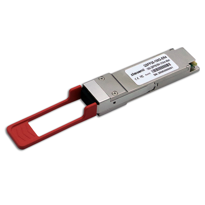
ZK-QSFP28-100G-ER4
100Gbps QSFP28 ER4 1310nm 40km SMF Transceiver
Features
n Compliant to Ethernet 100GBASE-ER4
n Supports 103.125Gb/s aggregate bit rate
n Transmitter: cooled 4x25Gb/s LAN WDM TOSA
(1295.56, 1300.05, 1304.58,1309.14nm)
n Receiver: 4x25Gb/s APD ROSA
n Up to 40km reach for G.652 SMF
n Built-in 4-channel Clock and Data Recovery
n (CDR) in TX and RX
n Duplex LC optical receptacle
n 4x25G electrical interface (OIF CEI-28G-VSR)
n RoHS-10 compliant and lead-free
n Single +3.3V power supply
n Maximum power consumption 4.5W Case operating temperature
Commercial: 0 ~ +70℃
Extended: -5 ~ +85℃
Industrial: -40 ~ +85℃
Applications
n 100GBASE-ER4 Ethernet Links
n Infiniband QDR and DDR interconnects
n Client-side 100G Telecom connections
Description
This product is a 100Gb/s transceiver module designed for optical communication applications compliant to Ethernet 100GBASE-ER4 standard. The module converts 4 input channels of 25Gb/s electrical data to 4 channels of LAN WDM optical signals and then multiplexes them into a single channel for 100Gb/s optical transmission. Reversely on the receiver side, the module de-multiplexes a 100Gb/s optical input into 4 channels of LAN WDM optical signals and then converts them to 4 output channels of electrical data.
The central wavelengths of the 4 LAN WDM channels are 1295.56, 1300.05, 1304.58 and 1309.14 nm as members of the LAN WDM wavelength grid defined in IEEE 802.3ba. The high- performance cooled LAN WDM DFB transmitters and high sensitivity APD receivers provide superior performance for 100Gigabit Ethernet applications up to 40km links.
The product is designed with form factor, optical/electrical connection and digital diagnostic interface according to the QSFP+ Multi-Source Agreement (MSA). It has been designed to meet the harshest external operating conditions including temperature, humidity and EMI interference.
Absolute Maximum Ratings
It has to be noted that the operation in excess of any individual absolute maximum ratings might cause permanent damage to this module.
Parameter | Symbol | Min | Max | Unit | Notes |
Storage Temperature | TS | -40 | 85 | ℃ | |
Power Supply Voltage | VCC | -0.3 | 4.0 | V | |
Relative Humidity (non-condensation) | RH | 0 | 85 | % | |
Damage Threshold | THd | -3.0 | dBm |
Recommended Operating Conditions
Parameter | Symbol | Min | Typical | Max | Unit | Notes |
Operating Case Temperature |
TOP | 0 | 70 |
℃ | Commercial | |
-5 | 85 | Extended | ||||
-40 | 85 | Industrial | ||||
Power Supply Voltage | VCC | 3.135 | 3.3 | 3.465 | V | |
Data Rate, each Lane | 25.78125 | Gb/s | ||||
Control Input Voltage High | 2 | Vcc | V | |||
Control Input Voltage Low | 0 | 0.8 | V | |||
Link Distance (SMF) | D | 40 | km | 1 |
Notes:
1. Depending on actual fiber loss/km (link distance specified is for fiber insertion loss of 0.35dB/km)
Pin Assignment and Pin Description
Pin | Symbol | Name/Description | Notes |
1 | GND | Transmitter Ground (Common with Receiver Ground) | 1 |
2 | Tx2n | Transmitter Inverted Data Input | |
3 | Tx2p | Transmitter Non-Inverted Data output | |
4 | GND | Transmitter Ground (Common with Receiver Ground) | 1 |
5 | Tx4n | Transmitter Inverted Data Input | |
6 | Tx4p | Transmitter Non-Inverted Data output | |
7 | GND | Transmitter Ground (Common with Receiver Ground) | 1 |
8 | ModSelL | Module Select | |
9 | ResetL | Module Reset | |
10 | VccRx | 3.3V Power Supply Receiver | 2 |
11 | SCL | 2-Wire serial Interface Clock | |
12 | SDA | 2-Wire serial Interface Data | |
13 | GND | Transmitter Ground (Common with Receiver Ground) | |
14 | Rx3p | Receiver Non-Inverted Data Output | |
15 | Rx3n | Receiver Inverted Data Output | |
16 | GND | Transmitter Ground (Common with Receiver Ground) | 1 |
17 | Rx1p | Receiver Non-Inverted Data Output | |
18 | Rx1n | Receiver Inverted Data Output | |
19 | GND | Transmitter Ground (Common with Receiver Ground) | 1 |
20 | GND | Transmitter Ground (Common with Receiver Ground) | 1 |
21 | Rx2n | Receiver Inverted Data Output | |
22 | Rx2p | Receiver Non-Inverted Data Output | |
23 | GND | Transmitter Ground (Common with Receiver Ground) | 1 |
24 | Rx4n | Receiver Inverted Data Output | 1 |
25 | Rx4p | Receiver Non-Inverted Data Output | |
26 | GND | Transmitter Ground (Common with Receiver Ground) | 1 |
27 | ModPrsl | Module Present | |
28 | IntL | Interrupt | |
29 | VccTx | 3.3V power supply transmitter | 2 |
30 | Vcc1 | 3.3V power supply | 2 |
31 | LPMode | Low Power Mode | |
32 | GND | Transmitter Ground (Common with Receiver Ground) | 1 |
33 | Tx3p | Transmitter Non-Inverted Data Input | |
34 | Tx3n | Transmitter Inverted Data Output | |
35 | GND | Transmitter Ground (Common with Receiver Ground) | 1 |
36 | Tx1p | Transmitter Non-Inverted Data Input | |
37 | Tx1n | Transmitter Inverted Data Output | |
38 | GND | Transmitter Ground (Common with Receiver Ground) | 1 |
Notes:
1. GND is the symbol for signal and supply (power) common for QSFP28 modules. All are common within the QSFP28 module and all module voltages are referenced to this potential unless otherwise noted. Connect these directly to the host board signal common ground plane.
2. VccRx, Vcc1 and VccTx are the receiving and transmission power suppliers and shall be applied concurrently. Recommended host board power supply filtering is shown below. Vcc Rx, Vcc1 and Vcc Tx may be internally connected within the QSFP28 transceiver module in any combination. The connector pins are each rated for a maximum current of 1000mA.
Electrical Characteristics
The following electrical characteristics are defined over the Recommended Operating Environment unless otherwise specified.
Parameter | Symbol | Min. | Typ. | Max | Unit | Notes |
Power Consumption | p | 4.5 | W | |||
Supply Current | Icc | 1360 | mA | |||
Transmitter (each Lane) | ||||||
Input differential impedance | Rin | 100 | Ω | |||
Differential Termination Mismatch | 10 | % | ||||
Differential Data Input Amplitude | Vin, PP |
180 | 1000 | mV | ||
LPMode, Reset and ModSelL | VIL | -0.3 | 0.8 | V | ||
VIH | 2 | Vcc+0.3 | V | |||
Receiver | ||||||
Differential Data Output Amplitude | Vout, PP |
350 | 900 | mV | ||
Differential Termination Mismatch | 10 | % | ||||
Transition Time, 20 to 80% | 9.5 | ps | ||||
ModPrsL and IntL | VOL | 0 | 0.4 | V | ||
VOH | Vcc-0.5 | Vcc+0.3 | V | |||
Optical Characteristics
The following optical characteristics are defined over the Recommended Operating Environment unless otherwise specified.
Parameter | Symbol | Min. | Typical | Max | Unit | Notes |
Transmitter | ||||||
Lane wavelength(range) | L0 | 1294.53 | 1295.56 | 1296.59 | nm | |
L1 | 1299.02 | 1300.05 | 1301.09 | nm | ||
L2 | 1303.54 | 1304.58 | 1305.63 | nm | ||
L3 | 1308.09 | 1309.14 | 1310.09 | nm | ||
Signaling rate, each lane | 25.78125 | GBd | ||||
Side-mode suppression ratio | SMSR |
30 | ||||
Total launch power | PT | 10.5 | dBm | |||
Average launch power, each lane | Pavg |
-2.9 |
4.5 | dBm | ||
OMA, each Lane | POMA | 0.1 | 4.5 | dBm | ||
Extinction Ratio | ER | 4 | dB | |||
Difference in Launch Power between any Two Lanes (OMA) | Ptx,diff | 3.6 | dB | |||
Transmitter and Dispersion Penalty, each lane | TDP | 2.5 | dB | |||
OMA minus TDP, each lane | OMA-T DP |
-0.65 | dBm | |||
Average launch power of OFF transmitter, each lane | Poff | -30 | dBm | |||
Transmitter reflectance | RT | -12 | dB | |||
RIN20OMA | RIN | -130 | dB/Hz | |||
Optical Return Loss Tolerance | ORLT | 20 | dB | |||
Transmitter eye mask {X1,X2,X3, Y1, Y2, Y3} | {0.25, 0.4, 0.45, 0.25, 0.28, 0.4} | |||||
Receiver | ||||||
Signaling rate, each lane | 25.78125 | GBd | ||||
Average Receive Power, each Lane |
-20 |
-4.9 |
dBm | |||
Receive Power (OMA), each Lane |
-4.9 |
dBm | ||||
Receiver Sensitivity (OMA), each Lane | SEN1 |
-14.65 |
dBm | BER = 1x10-12 | ||
Receiver Sensitivity (OMA), each Lane | SEN2 |
-18.65 |
dBm | BER = 5x10⁻⁵ | ||
Receiver reflectance | -26 | dB | ||||
Difference in Receive Power between any Two Lanes (Average and OMA) |
Ptx,diff |
3.6 |
dB | |||
LOS Assert | LOSA | -35 | dBm | |||
LOS Deassert | LOSD | -20 | dBm | |||
LOS Hysteresis | LOSH | 0.5 | dB | |||
Digital Diagnostic Functions
The following digital diagnostic characteristics are defined over the normal operating conditions unless otherwise specified.
Parameter | Symbol | Min. | Max | Unit | Range |
Temperature monitor absolute error | DMI_ Temp | -3 | 3 | ℃ | 0~85℃ |
Supply voltage monitor absolute error | DMI _VCC | -3 | 3 | % | 0~Vcc |
RX power monitor absolute error | DMI_RX | -3 | 3 | dB | -5~-20dBm |
Bias current monitor error | DMI_ bias | -10 | 10 | % | 0~100mA |
TX power monitor absolute error | DMI_TX | -3 | 3 | dB | -2.9~4.5dBm |
Mechanical Dimensions
Important Notice
Performance figures, data and any illustrative material provided in this data sheet are typical and must be specifically confirmed in writing by Zkosemi before they become applicable to any particular order or contract. In accordance with the Zkosemi policy of continuous improvement specifications may change without notice. The publication of information in this data sheet does not imply freedom from patent or other protective rights of Zkosemi or others. Further details are available from any Zkosemi sales representative.